

DRC, LVS, and RCX
Authors: Michael Cunningham, Joseph Chong, and Dr. Dong S. Ha
Layout Design Process
- Suggested steps for layout design:
a. Place components and run DRC for spacing. Fix any issues.
b. Connect the devices following the rules as best as possible.
c. Run LVS to verify connectivity. Fix any issues.
d. Run DRC and resolve all errors (with the exception of density errors that do not directly affect your actual circuit).
e. Run RCX and simulate (Post Layout Simulation).
f. If design needs to be improved, return to step (a) or (b) and fix any connections or placements that degrade performance. Continue with steps (c), (d), (e), and (f).
g. Once satisfied, add in the dummy layers to resolve final density errors. Re-extract and simulate for final design.
Running the Design Rule Checker (DRC)
- Once you have placed your devices, it's a good idea to run the Design Rule Checker (DRC) before routing everything. Essentially, the DRC will check to make sure that the layout you have made is possible to fabricate according to the foundry rules.
- The PDK we are using requires the use of Calibre, that's why we had to adjust the setup (in the layout tutorial). In the layout window, go to Calibre → Run DRC.
- If you have already created the runset, skip to Step 11. Otherwise, close the "Load Runset File" form.
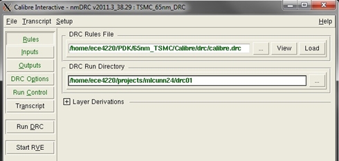
- In the interactive window, select the "Rules" tab and type (or copy and paste) the following text into the "DRC Rules File" box. Then, select "Load".
NOTE: To paste in Calibre, use "Ctrl + v".DRC Rules File: /home/ece4220/PDK/65nm_TSMC/Calibre/drc/calibre.drc
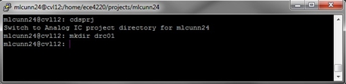
- In your terminal, we will make a directory for the drc information to be stored.
a. Type in "cdsprj"
b. Type "mkdir drc01"
- Change your "DRC Run Directory" to this location so you don't flood your project space with drc files.
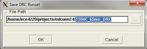
- Let's save this runset. Go to File → Save Runset.
- With the "File Path" empty, press OK.
- In the next window, give it a name (e.g. TSMC_65nm_DRC). Select OK.
Close "Calibre Interactive" and then re-open it (Calibre → Run DRC).
Load a Runset
- Load the runset we just created.
- Clock on the "Inputs" tab and verify that the file information is correct.
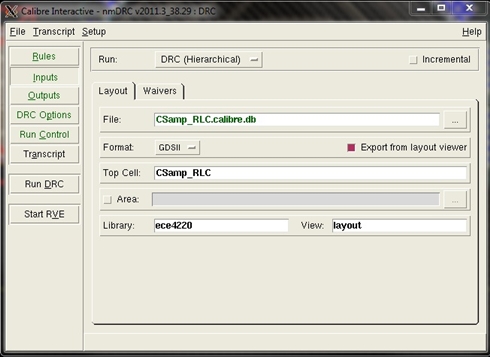
- Now, select "Run DRC".
Once it is complete (which may take a while, even on campus), a summary file and the Results Viewing Environment (RVE) window will appear.
It is important to note that even though there are a lot of errors, often one fix will solve many other problems.
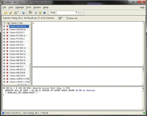
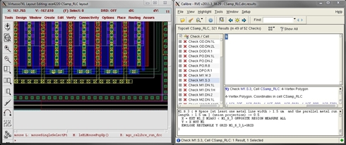
DRC Debugging
- Go to the RVE window. Here, there is a list of errors and a description in the bottom box. We will only focus on/disregard the following as mentioned:
a. All "CSR.*" (Corner Stress Relief) errors can be ignored. Metals and vias are not allowed in chip corners, but we are not creating the entire chip.
b. Any "*.EN" (Enclosure) errors regarding chip edge can be waived; all others should be resolved according to the rule described in the explanation window.
c. All "*.S" (Spacing) errors should be resolved. Move metals or vias to meet the minimum spacing requirements.
d. All "*.W" (Width) errors should be resolved. Resize any flagged objects to meet the maximum/minimum width rules.
e. All "*.A" (Area) errors should be resolved. Resize the metal/via as described in the check.
f. All "G.*" (Grid) errors should be resolved. The grid is the minimum resolution that can be manufactured. If you used paths with variable ends and specified a length less than the grid resolution (for some unknown reason), you will receive an error. All other path ends are fixed to the grid.
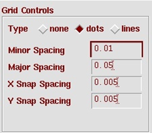
Additionally, do not change the grid resolution from 0.005 in the layout display options ("e").
g. All "IND.DN" (Inductor Density) errors can be waived as this is one segment of a chip. This error is generated if the inductor is too large compared to the chip.
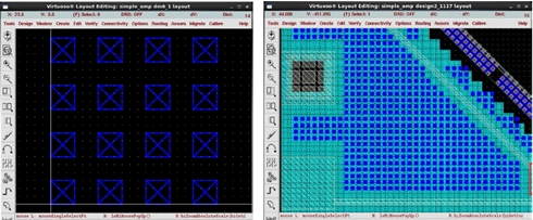
h. All ".DN" (Density) errors should be resolved (with the exception of the aforementioned case). Certain metal and oxide densities are required for fabrication. TSMC recommends their autofill script, but I will not cover this as it is better suited for those with sufficient layout experience.
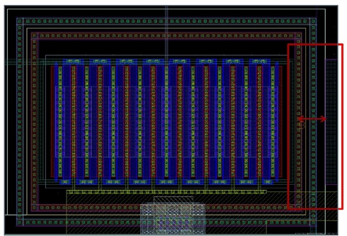
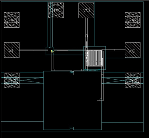
Alternatively, you can satisfy this error by manually adding in dummy layers of metal - Mx(dm) - thin oxide for device - OD(dm) - and polysilicon oxide - PO(dm) in the empty areas of your chip. This image below is a 4 x 4 array of dummy layers OD, PO, M1, M2, M3, M4, M5, and M6 vertically aligned. Each square is 3μm x 3μm with 3μm spacing.
- Once you select a check/cell in the left column, double-clicking or pressing the light button in the toolbar will highlight and zoom in on the error. Follow the description to resolve the error.
Layout vs. Schematic (LVS)
- We run LVS to check that our layout is correctly setup (to see if we missed/added something) when compared to the schematic. It is important that both have the same components/connections.
- Fire we have to add some files:
a. In the terminal paste/type the following line:Terminal Code (case sensitive): cp -r $TSMCPDK_HOME/{Assura,assura_tech.lib} .
b. Now, in the terminal paste/type:Terminal Code (case sensitive): echo "DEFINE avTech \$ASSURAHOME/tools/assura/etc/avtech/avTech">>cds.lib
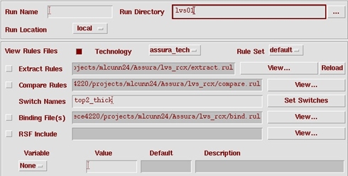
- In the layout window, go to Assura → Run LVS....
- Switch the technology to assura_tech next to the "View Rules Files" section and type in a name for the "Run Directory" (e.g. "lvs01").
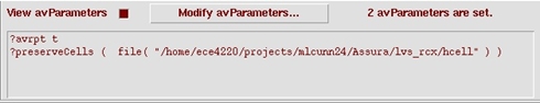
- Also, click on "Modify avParameters" and go to "?preserveCells".
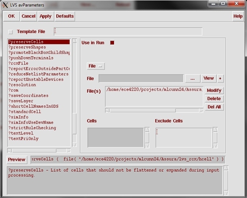
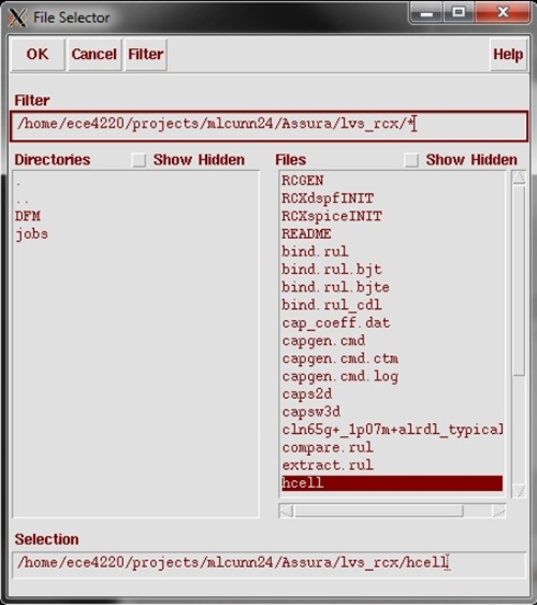
- Browse the files ("...") and double-click on Assura → lvs_rcx, then double-click on hcell (in the "Files" column).
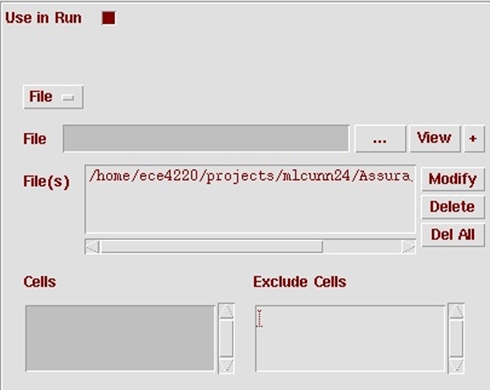
- Select "+" on the right, check the "Use in Run" square, and then select OK. It should be added to the avParameters in the original window at the bottom.

Run LVS
- Run LVS by selecting OK (it's fine to overwrite the last run if you don't plan on using the previous data). A progress box will appear in the lower right-hand section of your screen. If it takes a very long time, you will most likely have errors (or limited server space).
Debugging with LVS
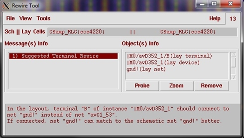
- If you run LVS and you receive a message like the one below, you have some issues. Select OK.
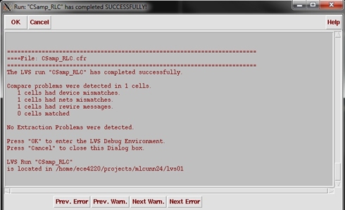
- A debug window should appear. If not, go to Assura → LVS Debug Env... to open the debugger.
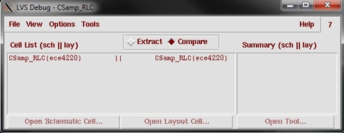
- In the debugger, select one of the cell list items and a summary of the issues will appear to the right.
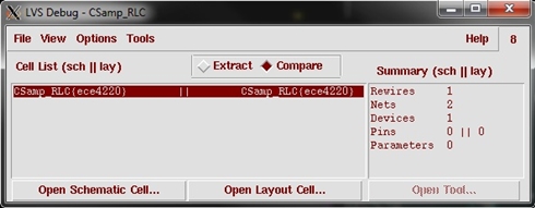
- A few mismatches are shown, but they could all be flagged form one error (in this case, I have forgotten to add a net). You can select each message summary and choose the "Open Tool..." option to easily find and debug.
a. Often "Rewires" will provide the clearest insight to the problem.
b. "Nets" is useful if you have completely forgotten a connection, but it will be shown in terms of net names which can be confusing.
c. "Devices" is most useful if you've forgotten a device in the layout or added one. ("Connectivity → Update → Device Correspondence" can be useful in linking a laylout device to a schematic device.)
d. "Pins" should be straightforward; missing, misnamed, or added.
e. "Parameters" is indicating that the parameters of a device in the layout do not match the corresponding device in the schematic. This is often fixed manually or with an automatic tool in the layout window ("Connectivity → Update → Layout Parameters" to change the layout to match the schematic or "Connectivity → Update → Schematic Parameters" to change the schematic to match the layout).
- If you select an error in the object info column, Zoom will focus the error in the layout and Probe will highlight the error in the schematic view. The message descriptions are also very useful in identifying the real issue. As an example, in the error below I have forgotten to connect the bulk of the MOSFET "M0" to ground ("gnd!").
- Once you think you've fixed the obvious errors, Re-run LVS. (You can save your design with the bindkey "F2").
NOTE: If you forgot to remove the probes before exiting the debug environment, go to Assura → Probing... and select "Remove All" at the bottom of the window.
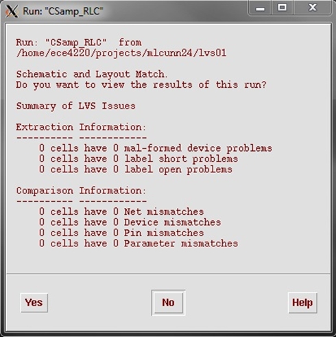
- Once you have successfully fixed any errors and your layout and schematic match, you will receive a single window with the summary. Select "No"; there is no need to view the results of a successful run.
RC Extraction (RCX or QRC)
- In order to get a good idea of realistic parameters in our design, we run RCX which can estimate and add to your design the parasitic resistances (R), capacitances (C), self inductances (L), and mutual inductances (K). We are only interested in RC parasitics.
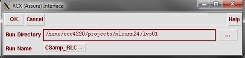
- In the layout window (Tools → Design Synthesis → Layout XL to open the layout view from the schematic window), go to Assura → Run RCX....
- Keep the "Run Directory" the same as the LVS run directory, make sure the run name is correct, and select OK. If you're unsure of the path, run LVS before RCX and it will be set automatically next time you run RCX.
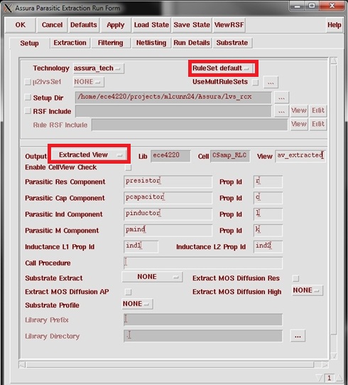
- The Assura Parasitic Extraction Run Form will appear.
In the Setup tab:
a. Change "Rule Set" to default.
b. Change "Output" to Extracted View.
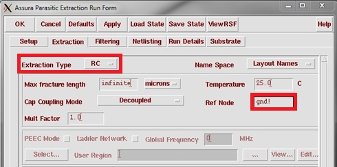
In the Extraction tab:
a. Change the "Extraction Type" to RC.
b. Change "Ref Node" to gnd! (if we had used a substrate connection it would be sub!).
c. Make sure the max fracture length is infinite, the coupling mode is decoupled, and multiplication factor is 1.0 (these should be the default).
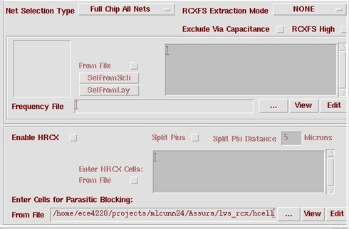
d. Next to "From File", select "..." and add hcell (Assura lvs_rcx; hcell is in the right column).
- Select OK. A progress form will appear in the lower right-hand corner or your screen.
- If your RCX failed, you may need to re-copy a folder as some files may be missing.
a. In the terminal type/paste the following:
Note: This should be in your main projects directory; e.g.
/home/ece4220/projects/your_user_id - type pwd to print your working directory.Terminal Code (case sensitive): cp -r /home/ece4220/PDK/65nm_TSMC/Assura .
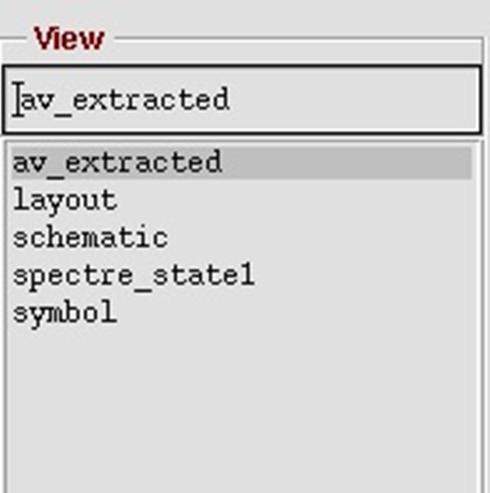
- Once the extraction finished, you should see an "av_extracted" view in your library manager for the cell.
- You are now ready to start the Post Layout Simulation tutorial.
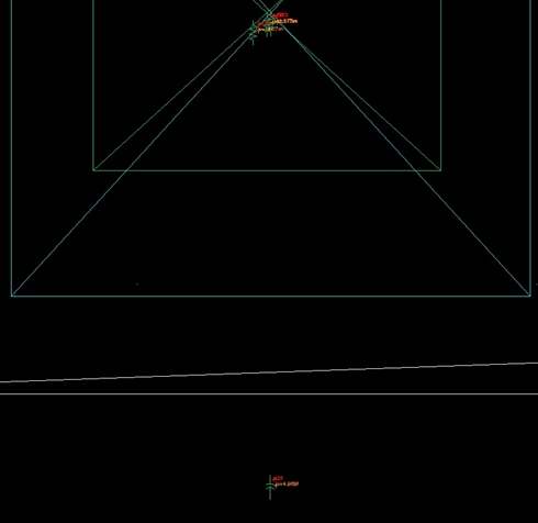
Note: If you open the av_extracted view, you can see the parasitic extraction in detail. If you zoom in close enough, you can see the values.

MICS IAP Members


