

Layout Component Placement
Authors: Michael Cunningham, Joseph Chong, and Dr. Dong S. Ha
Generating I/O pads and components
1. Open the schematic you wish to generate a layout of (it should be the one with pin connections).
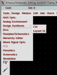
2. Go to Tools → Design Synthesis → Layout XL.
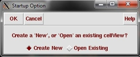
3. If this is the first time generating a layout, select Create New and OK. If you already have a layout, then open the existing one.
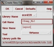
4. In the next dialog box, keep the name the same but make sure that the "View Name" is "layout". Select OK.
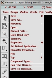
5. A new window and the Layer Selection Window (LSW) will open. In the layout window, go to Design → Gen From Source... .
6. An options form will open.
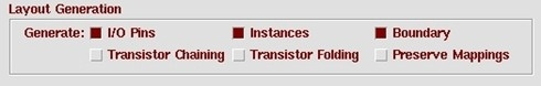
a. Layout Generation – select I/O Pins, Instances, and (optionally) Boundary
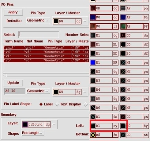
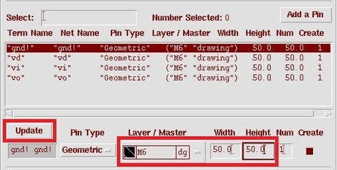
b. I/O Pins
i. Highlight all the terminal names
ii. In the Layer/Master below the names, select M6(dg).
iii. Change the width AND height to 50.0 .
iv. Update .
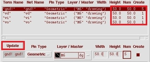
v. Highlight the "gnd! " terminal
vi. Change the "Num " to "5 ". Update
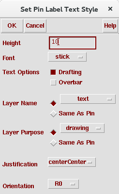
c. I/O pad labels: Choose “Label” for “Pin Label Shape”, Click on “Pin Label Options” and set the “Height” to “10”. Click OK.
d. Select OK.
NOTE: When designing a chip that will need to be measured with probes, more ground pads are generated to form a ground/signal/ground connection or ground/signal/signal/ground (for differential) to mimic the connections.
Identifying layout components and pin locations
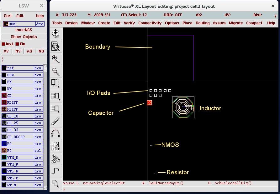
1. After generating from source, you will have a layout window with the components and pads, and a layer select window (LSW). Generally you need to place all your components in the right upper quadrant within the boundary. However, since the boundary is an auto-calculated area estimation, its size is just for your reference.
Note: when you select component in schematic window, it will be highlighted in both windows. If you've closed your schematic, you will need to close layout and reopen it through the schematic in order to retain the link between windows.
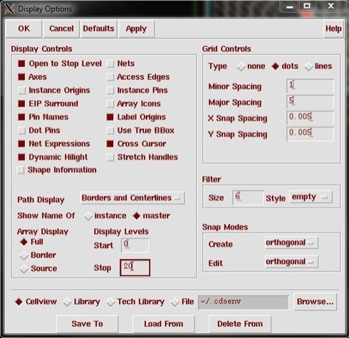
2. In the layout, press "e" to open the display options.
a. Select Pin Names to show component pin names. This will be useful for MOSFETs.
b. Change the Display Levels starts at 0 and stops at some number such as 5~20. This will allow you to view inside a component.
c. Make sure X and Y snap spacing is 0.005 or multiple of it. Use multiples, such as 0.01 or 0.015 or larger, if you’re dealing with large components.
d. Enable “Nets” to show net connection, but it may be confusing.
e. Select “Library” at the bottom row and click “Save To” button. The setting is now saved to your library and applies to all layouts in your library.
3. Right-clicking your mouse and drag and area to zoom-in. Ctrl+z to zoom in to the middle, and Shift+z to zoom out. “f” to fit all.
4. Identify the MOSFET and zoom in. You will see that it consists of four pins: D/G/S/B. The text color of the pin name and the metal color of the pin will give you a hint of what metal layer it is located. Comparing with the color shown in LSW, you will identify the M3 loop is the G connection, the S is the M4 rectangle in the middle, D is M2 at the bottom, and B is an M1 loop.
NOTE: We’re using a pre-defined RF NMOS because: (1) MOSFET area is not our concern; (2) the frequency response of the MOSFET is mostly characterized by the foundry. We will only work on interconnecting the MOSFET with other components.
5. You may use the LSW and turn layers visible / invisible to look at different layers. “AV” means all visible, and “NV” means none visible. Select appropriate visible layers in LSW, then click on layout window, and press “Ctrl+R” to redraw (refresh).
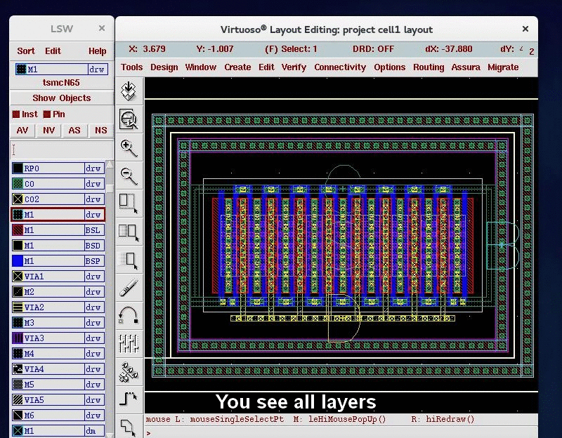
Figure 14. How to use LSW to turn layers visible / invisible.
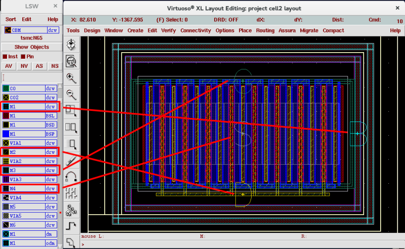
6. You may go through different layers of metals and vias as shown below. This will give you a clear view of the component.
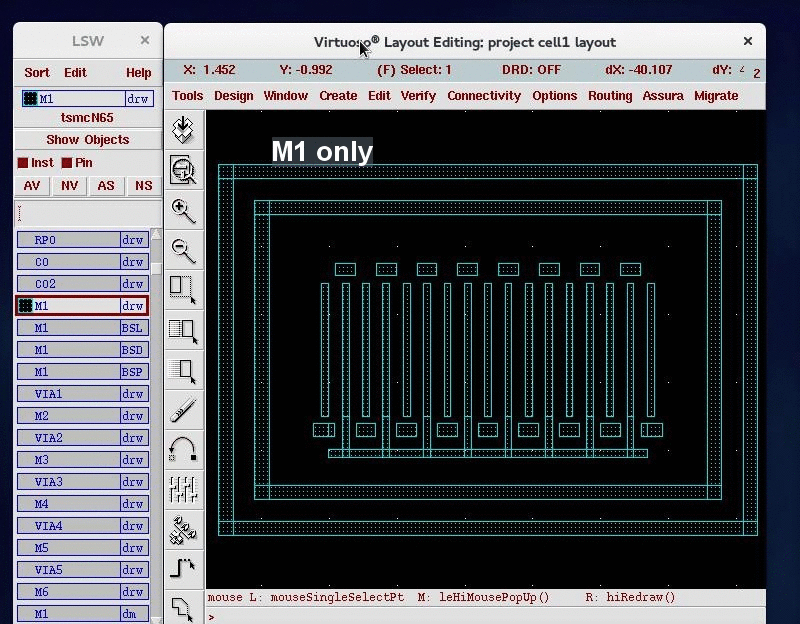
Figure 15. Layer by layer view of a MOSFET.
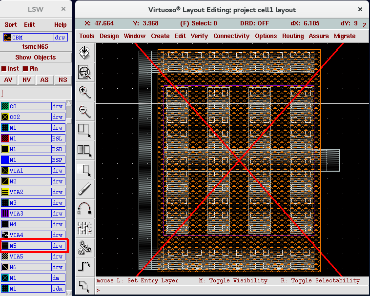
7. An example of metal-insulator-metal capacitor is shown. You may notice there are two sections of M5 according to its color. The other layers are capacitor top metal CTM (purple) and capacitor bottom metal CBM (orange), which are connected with VIA4 from M5. You may connect to the capacitor with M5 from the side or M6 from top. Check out its cross section from the layout lecture slides.
8. You may find that capacitors and resistors doesn’t show their pin names. But since they’re not polarized, we could just reverse the component in schematic if you connected it in reverse.
Placing the layout components
1. Now that you have figured out the location of pins for the components, you develop a floorplan for all your components in the layout.
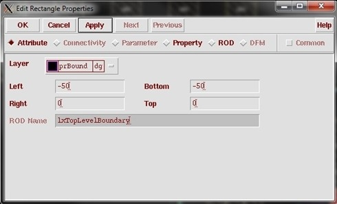
2. (Optional) If you have included the boundary in generation, you may resize it so it doesn’t interfere with the placement procedure.
a. Select the prBoundary (violet square) and press "q".
b. Adjust the dimensions as shown below.
3. Now place all the devices in the same general region (near the [0, 0] axis).
a. Press "Ctrl + a" to highlight everything. (The resistor is very small.)
b. Now press "m" and then select any devices that are far away (right click and enclose with a selection box, then click on it).
c. Move it closer to the other devices.
4. Consider I/O pad arrangements.
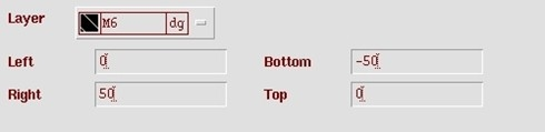
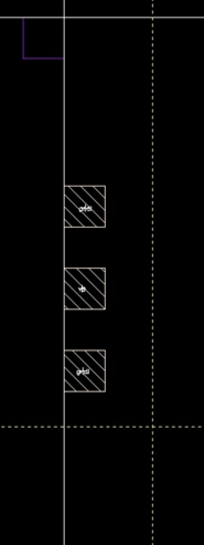
5. Now let's arrange our pads for G-S-G with a pitch of 100μm (center to center distance). This is just an example for a probe of pitch of 100 μm.
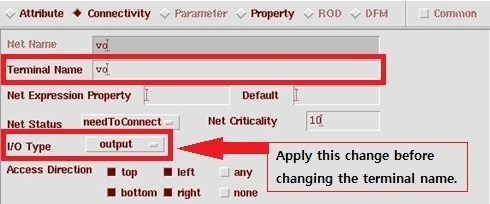
a. Select a "gnd!" pad and press "q". If you're unsure of which pad is which, the terminal name will be under the connectivity tab in the properties menu ("q").
b. Adjust the attributes as shown below.
c. Move the text over to the pad.
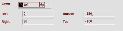
d. Now, do the same thing for the signal pad with a top/bottom spacing 100 units below.
e. Again, move the pin name over to the pad.
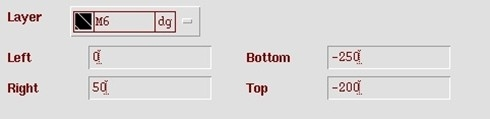
f. Finally, select another ground pad and place it 100 units below the signal pad.
g. Now select these pads and move them down about midway of your intended chip side.
h. Repeat this procedure for the output pad "vo " and place it on the right side.
PRO TIP : Simply copy the three pads (select them and press "c ") and place them. Then select the signal pads, press "q ", go to "Connectivity ", and change the terminal name to the new pad ("vo " in this case). However, you need to apply the correct I/O type before you can change the name. Once finished, delete any duplicate pads (and don't forget to change the text name).
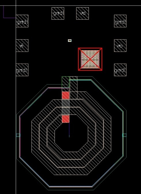
6. Place the rail and additional ground pad at the top with the same spacing. The distance between different pads depends on the method of measurement (probes or bondwires) and its size. For this tutorial, assume we can place it anywhere in the middle with 100 μm pitch to pitch distance between the gnd! and vd pads.
7. Place all your components. You move the components to appropriate location and rotate them appropriately to potentially ease the latter routing process.
E.g. (1), the inductor, capacitor, and the drain node of transistor faces each other for easier connection.
E.g. (2), the source of transistor and the resistor are placed together for easier connection.
E.g. (3), the gate of the transistor should be easily accessible from the vi pad.
8. Below are some techniques for placing devices.
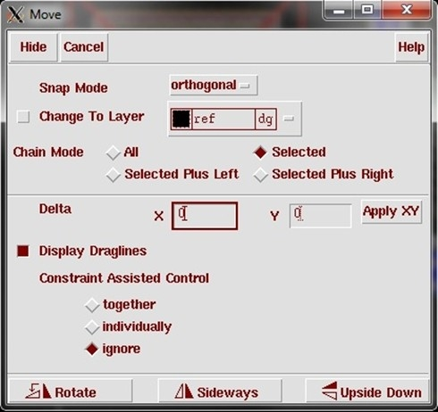
a. Select a device and press "m" to move it. The default is orthogonal movements which is useful for lining up edges (in conjunction with other techniques).
b. To rotate/flip/move a device, press "m" then "F3" and select the desired operation. You can also change the snap mode here. (Right clicking while in a move will also rotate the shape.)
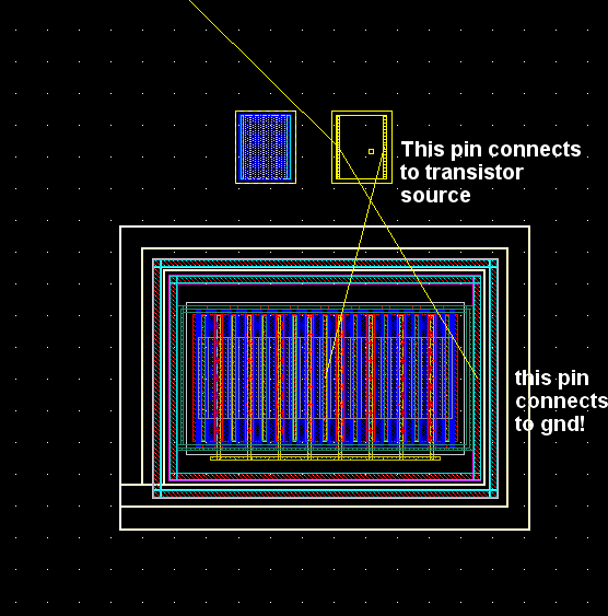
9. If you have started up layout with the Tools à Design Synthesis à Layout XL process, you’ll find guiding lines show up when you move a component. These are the pins that are interconnected. For example, when a resistor is moved as shown below, a line connects the resistor with the transistor S pin, and another line connects the resistor, trasistor B pin, and gnd! pad somewhere off the figure.
10. Usually pads are placed on opposite ends of the chip since the probes/connectors are much larger than the pads and require much more space. It is not a requirement that you do this in this tutorial (though we've already covered the steps).

MICS IAP Members


