

Layout
Authors: Michael Cunningham, Ji Hoon Hyun, Dr. Dong S. Ha
Environment Setup
- Since the design rule checker (DRC) needs to be run with calibre, we need to make an adjustment to the setup.
- First we need to copy the initialization file into your directory.
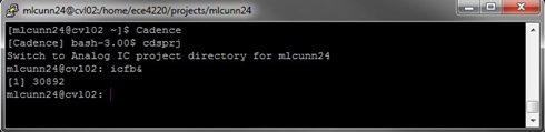
a. Log in to the CVL
b. Change your directory to cdsprj
c. Type the following line (or copy and paste it into the terminal (right click)).
Terminal Code (case sensitive): cp /home/ece4220/.cdsinit .
d. Now exit the cdsprj directory by typing in "exit".
- When starting Cadence, the sequence will now be
e. Cadence
f. cdsprj
g. icfb&
This will allow the file in cdsprj to overwrite the defaults of the Cadence initialization.
Generating a Layout
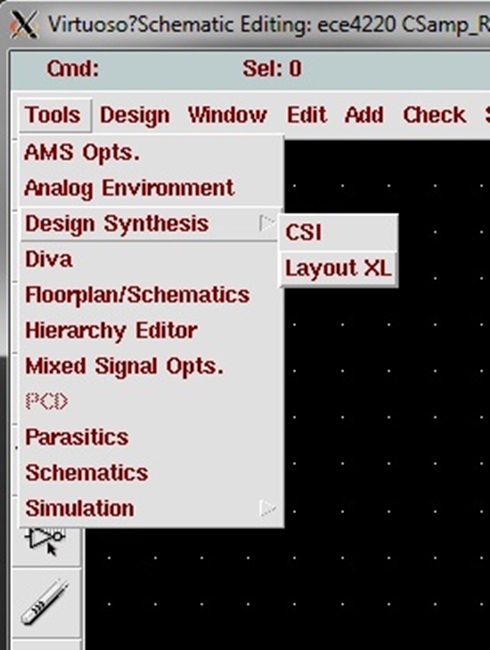
- Open the schematic you wish to generate a layout of (it should be the one with pin connections).
- Go to Tools → Design Synthesis → Layout XL.
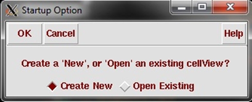
3. If this is the first time generating a layout, select Create New and OK. If you already have a layout, then open the existing one.
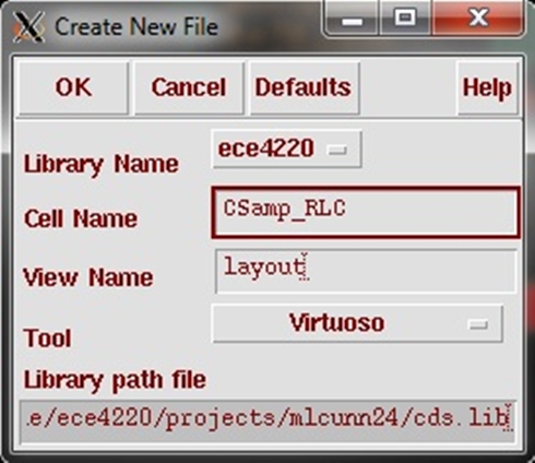
4. In the next dialog box, keep the name the same but make sure that the "View Name" is "layout". Select OK.
5. A new window and the Layer Selection Window (LSW) will open. In the layout window, go to Design → Gen From Source... .
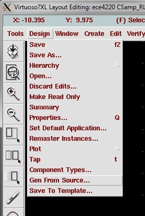
6. An options form will open.
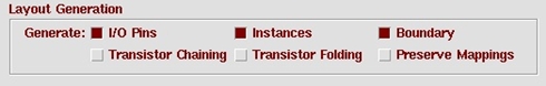
a. Layout Generation - select:
i. I/O Pins
ii. Instances
iii. Boundary
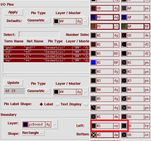
b. I/O Pins
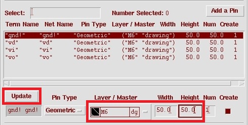
i. Highlight all the terminal names
ii. In the Layer/Master below the names, select M6(dg).
iii. Change the width AND height to 50.0.
iv. Update.
v. Highlight the "gnd!" terminal
vi. Change the "Num" to "5". Update.
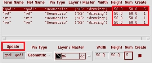
c. Select OK.
NOTE: When designing a chip that will need to be measured with probes, more ground pads are generated to form a ground/signal/ground connection or ground/signal/signal/ground (for differential) to mimic the connections.
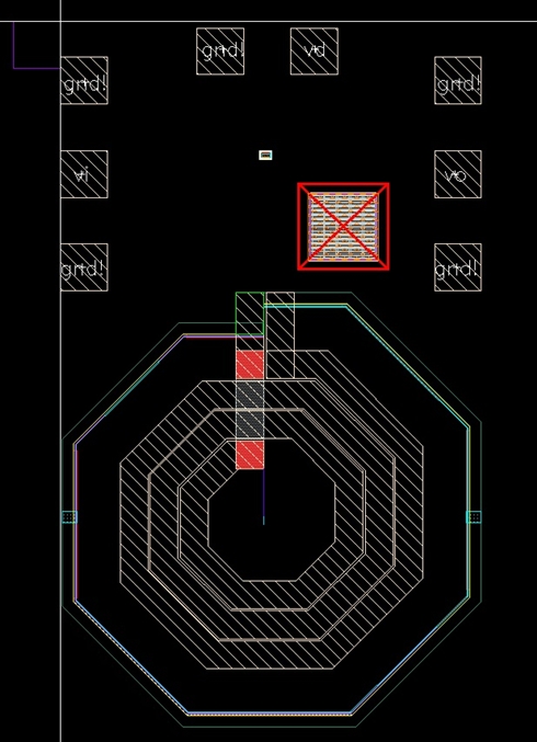
Placing the Layout Components
1. You should have the schematic window open with the layout window. You'll notice that if a component is selected in either one, it will highlight in both windows.
2. If you've closed your schematic, you will need to close layout and reopen it through the schematic in order to retain the link between windows.Go to Tools → Design Synthesis → Layout XL, Open Existing, OK, select the layout view name, OK.
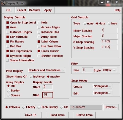
3. In the layout, press "e" to open the display options. Select Pin Names and Cross Cursor. These settings will help in layout, but are not required. You may change the Display Levels starts at 0 and stops at 20.
4. The first (and usually longest) part of layout is to place your devices (develop a floorplan). The complicated part is following the design rules of the foundry while taking into consideration the effects of placing devices in certain places/next to other components. Luckily, we are using developed models so you won't need to design them.
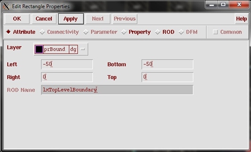
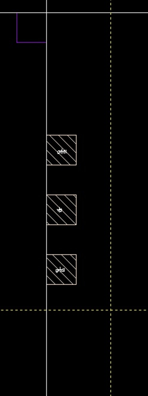
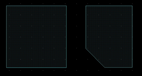
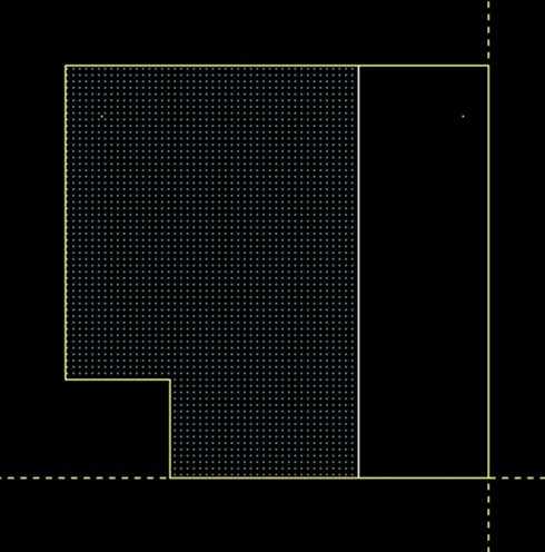
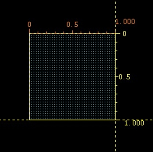
5. First. Let's move the "Place and Route Boundary" out of the way.
a. Select the prBoundary (violet square) and press "q".
b. Adjust the dimensions as shown below.
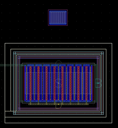
6. Now place all the devices in the same general region (near the [0, 0] axis).
c. Press "Ctrl + a" to highlight everything. (The resistor is very small.)
d. Now press "m" and then select any devices that are far away (right click and enclose with a selection box, then click on it).
e. Move it closer to the other devices.
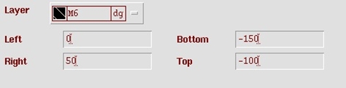
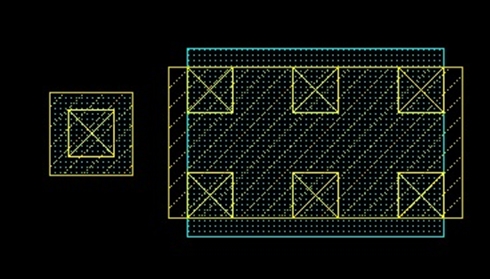
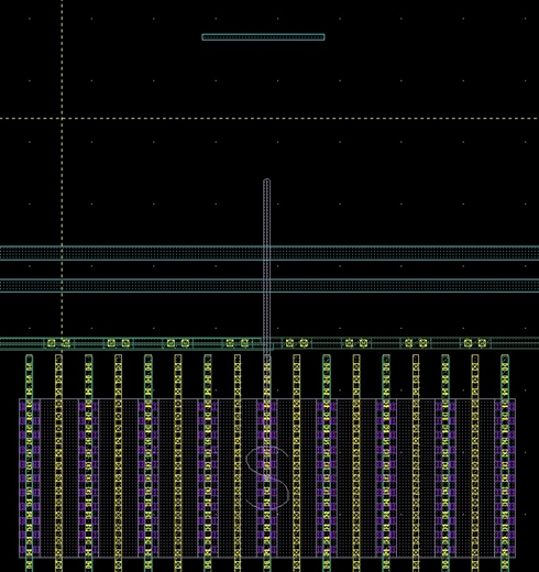
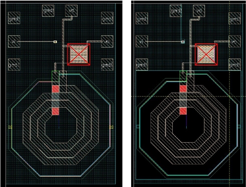
7. Now let's arrange our pads for G-S-G with a pitch of 100μm (center to center distance).
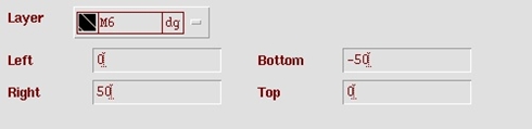
a. Select a "gnd!" pad and press "q". If you're unsure of which pad is which, the terminal name will be under the connectivity tab in the properties menu ("q").
b. Adjust the attributes as shown below.
c. Move the text over to the pad.
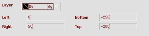
d. Now, do the same thing for the signal pad with a top/bottom spacing 100 units below.
e. Again, move the pin name over to the pad.
f. Finally, select another ground pad and place it 100 units below the signal pad.
g. Now select these pads and move them down about midway of your intended chip side.
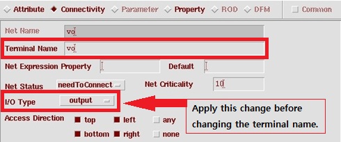
h. Repeat this procedure for the output pad "vo" and place it on the right side.
PRO TIP: Simply copy the three pads (select them and press "c") and place them. Then select the signal pads, press "q", go to "Connectivity", and change the terminal name to the new pad ("vo" in this case). However, you need to apply the correct I/O type before you can change the name. Once finished, delete any duplicate pads (and don't forget to change the text name).
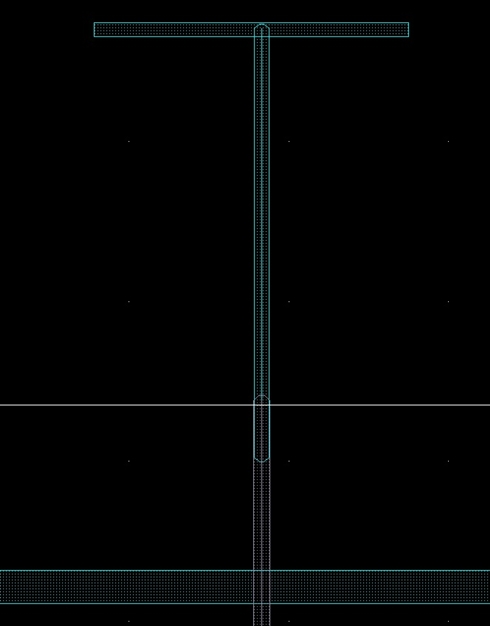
i. Place the rail and additional ground pad at the top with the same spacing.
j. Place all your components (some tips are in the following steps).
NOTE: If you want to resize the text, select all the text boxes, press "q", select the "Common" box on the upper right, and then change the "Height" to something like 15.
8. The bindkeys for layout will be very helpful. Below are some techniques for placing devices.
a. Pressing "F3" after pressing a bindkey will display the full options of that key.
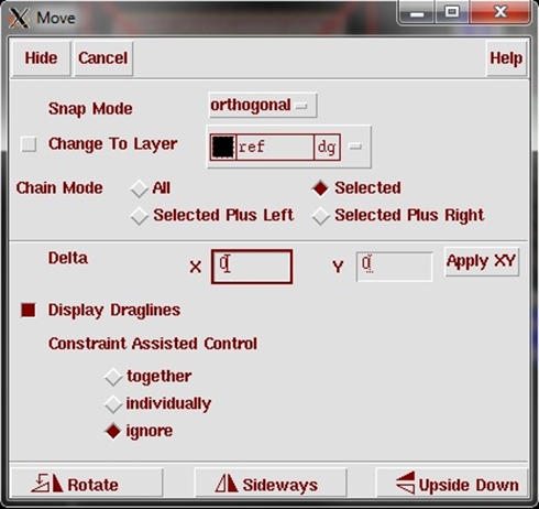
b. Select a device and press "m" to move it. The default is orthogonal movements which is useful for lining up edges (in conjunction with other techniques).
c. To rotate/flip/move a device, press "m" then "F3" and select the desired operation. You can also change the snap mode here. (Right clicking while in a move will also rotate the shape.)
d. In the option form ("e"), toggling on "Nets" can help for initial placement. This will mark the needed connections with lines.
e. You want to take up as little area as possible with minimal need for routing.
f. Usually pads are placed on opposite ends of the chip since the probes/connectors are much larger than the pads and require much more space. It is not a requirement that you do this in this tutorial (though we've already covered the steps).
Routing
Routing is important in layout. We don't want to add too many extra parasitic, but the metal interconnects must also provide a good connection.
Below is some useful information on routing and working in layout:
NOTE: keep an eye on the current function in the status bar on the bottom of your screen.

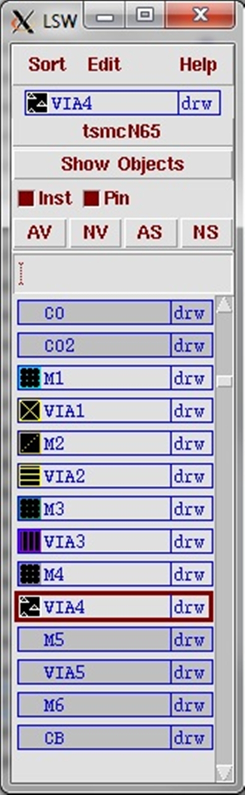
Layer Selection Window (LSW)
It is important to know what layer you are working on. Refer to the LSW window to navigate the layers. Since we are only routing metal interconnects, you will only be interested in the drw layers of metal 1 to metal 6 (i.e.M1, VIA1, M2, VIA 2, ..., VIA5, and M6). Select the desired layer to work on. In the LSW, select Sort → By Purposeand scroll down to the M1 through M6drw layers.
a. Selecting NV will hide all the layers ("none visible") except the one you have selected. You can add more layers by selecting them.
b. Selecting AV will show all the layers ("all visible").
NOTE: You can individually toggle layer visibility by clicking the layer with the middle mouse button.
c. Selecting AS or NS will toggle the ability to select the layers. If a layer is unselected, it cannot be modified in the layout window. Right clicking on a layer toggles individual selectability.
IMPORTANT: To update the layout to reflect these changes, you will need to select the layout window and press "Ctrl + r" to refresh the page.
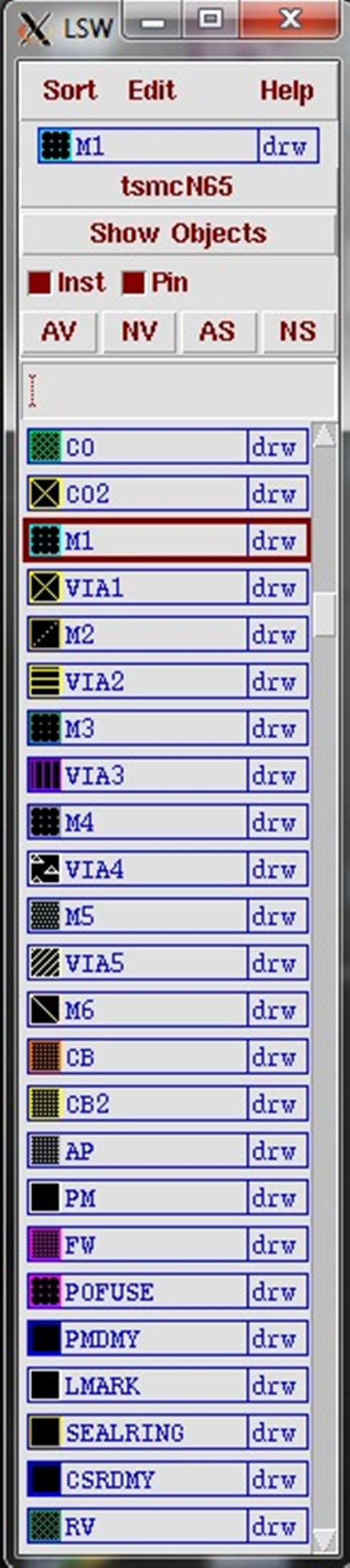
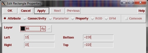
NOTE: If you need to change the layer of a metal line, select the shape and press "q". Under the attribute section you will have the option to change the layer to the appropriate dg layer.
Rectangles and Polygons
1. To create a rectangle, press "r". We can use these for paths and connections.
2. To create a polygon, press "Shift + p". This is useful for custom shapes (TSMC allows for 45 degree shapes).
DESIGN NOTE: We only use metal layers (not via layers) to travel across the board. It's always better to stay as low as possible in the metal layers, only moving into higher metal layers if necessary to traverse a path. Metal layer 6 is used mostly for pad contacting traces (providing inputs). Also try to avoid long, narrow paths as the metal layer exhibits a few mΩ/square.
Paths
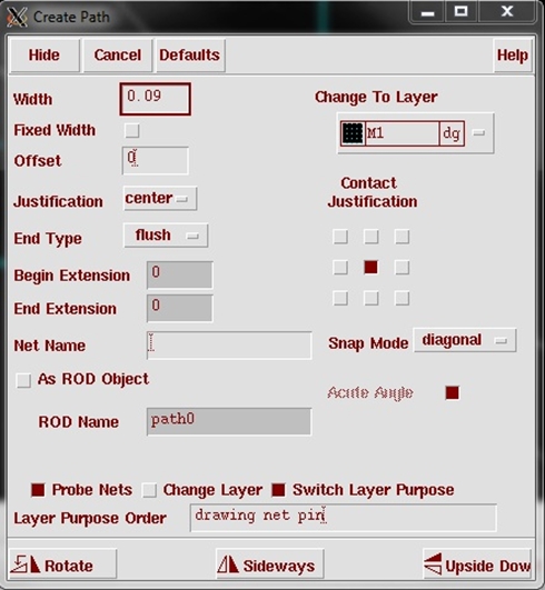
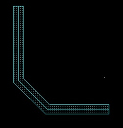
Paths are a special form of rectangles that make routing easier. To create a path, press "p". This creates a path on the selected layer and is very useful for long routes. If you open the path options ("F3") then you can adjust the "Snap Mode" to diagonal for more routing options. The width is usually a default width for the selected layer (which is fine to use).
Paths are simple to draw; click a starting point and click anytime you want to change direction. Press "Enter" (or double click) when you are finished.
BASIC METAL SIZE RULES (TSMC 65nm):
| Metal Layer | Width (μm) | Spacing | Sheet Resistance (Max) |
| M1 | 0.09 ≤ W ≤ 12.00 | ≥ 0.09 | 0.16 Ω/sq |
| Mx (x = 1,2,3,4,5,6,7) | 0.1 ≤ W ≤ 12.00 | ≥ 0.10 | 0.14 Ω/sq |
DESIGN TIP:
Note that these metal lines have a resistance associated with them. I have neglected the resistance in this tutorial, but you should be aware of the affects. The sheet resistance in the table above shows the maximum resistance (which occurs under minimum width and spacing but is a conservative value to use).
Recall:
R = ρ(l/A) = ρ(l/(tW)) = Rs(l/W) = (Sheet Resistance) * (Ratio)
The length-width ratio determines the number of squares. If you have a 100μm long line on metal layer 2 and it's only 0.1μm wide, then that is 100/0.1 = 1000 squares and 140Ω added to your path. This is one reason we like to limit the routing as much as possible.
Additionally, there are current limits associated with the metal lines so that we don't cause metal electromigration (which is analogous to too much water in a river - causing erosion, widening, etc.) which causes spots of higher resistance and changes in conductor dimensions; eventually this leads to failure¹. Current limits are also related to resistance (so that we don't drop too much voltage over the line).
Imax = J * W → (Metal Current Density) x (Line Width)
The voltage drop can be determined from the current and resistance of the line.
The table below tabulates the basic limitation of TSMC 65nm for 110°C junction temperature (nominal value) for long lines (over 20 microns). The max current will increase linearly for shorter lines up to 4 times (for lengths short than 5 microns).
Length scaled Imax: Imax ≤ (20μm / L) Imax ≤ 4Imax [5μm ≤ L ≤ 20μm]
| Metal Layer | Width (μm) | Imax (mA) |
| M1 | W | 1.51(W - 0.016) |
| Mx (x = 2,3,4,5,6,7) | W | 1.88(W - 0.016) |
Also of concern may be capacitance and propagation time associated with a path. The general capacitance relative to the ground plane is determined through the following equation (although proximity to other metal lines will increase this value).
C = Area * C''plate + Perimeter * C'fringe
Where one prime represents unit per meter, and double prime represents units per square meter.
The TSMC documentation provides capacitance using a different model. Typically, these values are in the aF to fF range. Exact values may be complicated to find so parasitic extraction is useful for determining line capacitance.
Keep in mind that the capacitance will increase for larger and longer lines as well as for close lines. The capacitance per square can be determined by dividing the value calculated above by the number of squares. The delay associated with this is approximately
td = 0.35RsqCsql²
¹ R.J. Baker, "The Metal Layers," in CMOS: Circuit Design, Layout, and Simulation, 3rd ed., Hoboken, NJ: Wiley, 2010, c. 3, sec. 2, pp. 63-70.
Contacts (Vias)
Vias are what we use to move between metal layers. They should fit within the metal layers (as shown below) and usually have strict rules on sizing and spacing. Newer versions of cadence have auto-via functions that make this task very simple. However, we only have a contact generator.
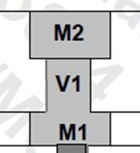
NOTE: The via layer is numbered the same as the metal layer that is directly below it.
To create a contact/via, press "o". Within the form there is drop down menu for contact type. If you want a single contact, select the option that lists the two surrounding layers. If you want to create an array, select the surrounding layers followed by a "c" and specify the dimensions. In this version, we can only generate layer-to-layer contacts (newer versions can generate via stacks). I recommend this feature to avoid sizing contacts.
IMPORTANT: Do not use the contact type with the "c" if you don't know what you are doing (or else you will probably receive a DRC error for having an edge less than the minimum width).
DESIGN TIP: You'll usually want to get at least two vias between layers for good contact and an array of at least 2x2 where possible to account misalignment in fabrication. Vias have an associated resistance associated with them, too. The number of vias should be increased to reduce the current (and voltage dropped) in each via. Multiple vias are essentially parallel resistances, so every via added will reduce the possibility of destroying the path. However, more than roughly six vias in one direction will usually be unnecessary (each via costs money, so overdesigning can become expensive).
The table below tabulates the basic limitation of TSMC 65nm for 110°C junction temperature (nominal value) for long lines (over 20 microns). The max current will increase linearly for shorter lines up to 4 times (for lengths shorter than 5 microns). Note that the scaling of vias uses the greater of the lengths between the metal layers it's connected to (the line that is limiting the max current).
Length scaled Imax: Imax ≤ (20μm / L) Imax ≤ 4Imax [5μm ≤ L ≤ 20μm]
where L is max[Lx,Lx+1] touching Vx
| Via Layer | Size | Rs | Imax (mA/via) |
| Vx (x = 1,2,3,4,5,6) | 0.10 x 0.10 μm² | 1.5 Ω/via | 0.158 |
| CO (Contact) | 0.09 x 0.09 μm² | 0.296 |
Chop and Stretch
Chop ("Shift + c") and stretch ("s") allow you to adjust rectangles and patsh by removing a piece (chop) or resizing an edge (stretch).
Merge
Merge ("Shift + m") is useful for joining separate, adjoining paths/rectangles into one.
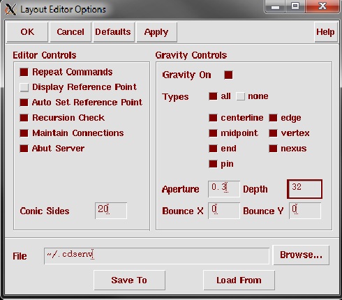
Gravity
Gravity is very useful for alignment and chopping; it snaps your cursor to corners and midpoints of other shapes. The bindkey "g" toggles gravity on and off. Press "Shift + e" to adjust settings. The aperture sets the distance away from an object that the cursor will snap. Therefore, a large value will snap the cursor at far distances and a small aperture will snap at closer distances. The depth determines how many levels down the snap can access. It ranges from 1 to 32. An aperture of "0.3" and depth of "32" should work fine. Bounce is not active as a default. Changes your .cdsenv file must be made; however, customization is not covered in this tutorial.
Ruler
The ruler ("k") is great for measuring specific distances (especially when coupled with gravity). Press "Shift + k" to clear all rulers.
Example of Routing
1. I need to route the source of the NMOS to the resistor.
2. I note that the source is on layer M4 and the resistor contact is on layer M1.
3. Go over to the LSW and select M1(drw). It might be helpful to Sort the layers by purpose.
4. Click NV, then select all the layers from M1 to M4 (and the via above M4 (i.e. VIA4) so we don't accidentally connect to any M5 lines).
5. Go to the layout window and refresh ("Ctrl + r"). Only the selected layers should be visible. (I've also added the M4 (pin) layer so that I can still see the pin name.)
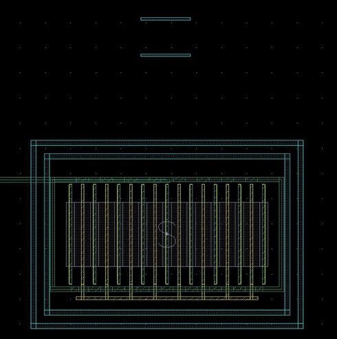
6. Now, in the LSW, select M4(drw).
7. Go to the layout window and press "p". Pick a point on the source and draw a path to a little outside the edges of the FET.
8. Now select M1(drw) and draw a path between this trace and the resistor (I've arranged my resistor to be contacted on the side closest to the transistor).
If you're unsure of what side is what, go to Connectivity → XL Probe and select the part of the device you want to see information about. It will tell you the plus/minus of the contact which should correspond with your schematic.
NOTE: If you attempt to start a path of one layer within a different layer, Layout XL will automatically switch your layer to the clicked-on layer. Two ways around this are to use rectangles to draw paths (keep in mind the metal width rules) or to stretch your patch to overlap after you draw it.
9. Now press "o" to open the contact form and select M2_M1c under the contact type.
10. Change the rows and columns to "2" for a 2x2 contact.
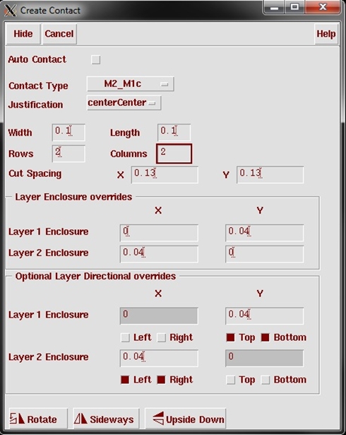
11. Place this contact at the overlap of the two metals. Repeat this step for M3_M2c and M4_M3c. I have made the M3_M2c contact layer 3v3 to avoid a stack of vias from the top layer to the bottom.
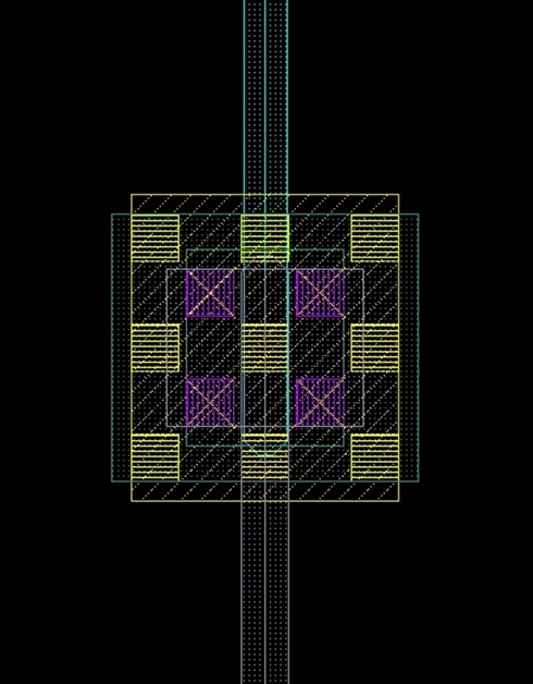
12. We have finished the route. Note that we do not need to add contacts to metals that touch the same layer; simply make sure they are overlapping.
13. Choose the next route and continue until you are finished.
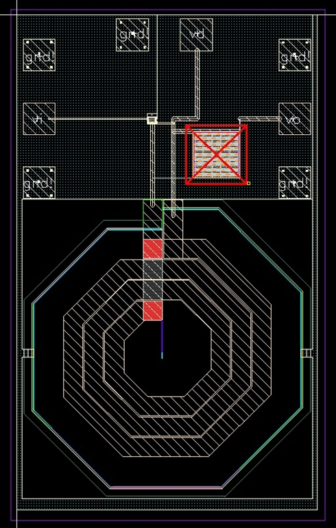
Ground Plane
It is fairly common to create a ground plane. This is simply a layer that is devoted to the ground signal (and we cut out areas where this layer is being used for other reasons).
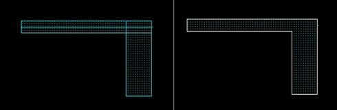
1. Let's choose M1 as our ground plane. Select M1 in the LSW and draw a rectangle that covers the entire circuit.
2. Select the layer you just drew and press "Shift + c" to activate chop.
3. Proceed to chop out the areas where the ground plane should not be.
4. Don't forget to attach the plane to the ground pad as well as any bulk connections (on the inductor sides and transistor). Note that the bulk of the transistor is tapped through the use of a guard ring.
NOTE: These FETs have a dual guard ring. The inner ring is P+ material and sits in the bulk - this is an NMOS bulk tap and should be tied to the negative supply voltage. The outer ring is N+ material and sits in an N-well. This is characteristics of PMOS guard rings and needs to be tied to the positive supply voltage to remain reverse biased (and draw out free carriers in the bulk).
It's usually bad design to put vias directly under pads, but you can decide if you want to do it here.
Finally add the prBoundary around this circuit (sizing doesn't matter, it just helps the software determine where things are; for instance, when using "Place As In Schematic"). Stretch ("s") is useful for this.
Design Rule Guide
Use the design rule guide provided by the foundry for more accurate requirements and more advanced design limitations.
IMPORTANT: The document is confidential and can result in legal consequences if the information is shared with anyone lacking permission to view it. DO NOT distribute the information to anyone.
A fairly good book (that is available electronically through the VT library) that covers CMOS circuit design, layout, and simulation is the following:
"CMOS: Circuit Design, Layout, and Simulation" (3rd ed.) by R. Jacob Baker (2010)

MICS IAP Members


