

Post Layout Simulation
Authors: Michael Cunningham, Ji Hoon Hyun, Dr. Dong S. Ha
Simulation
- Simulation is fairly simple, all you really need to do is switch to the av_extracted view:
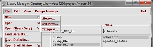
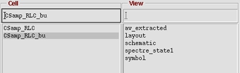
- Go to the Library Manager, select the testbench for your design and add a new cell view (File → New → Cell View...). You can also do this through the icfb window.
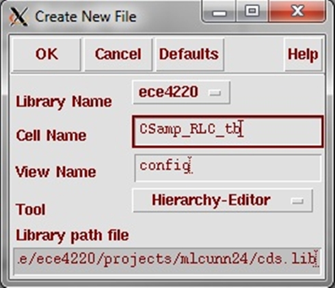
- In the next window, change the "Tool" to "Hierarchy-Editor". Make sure the "View Name" is now "config".
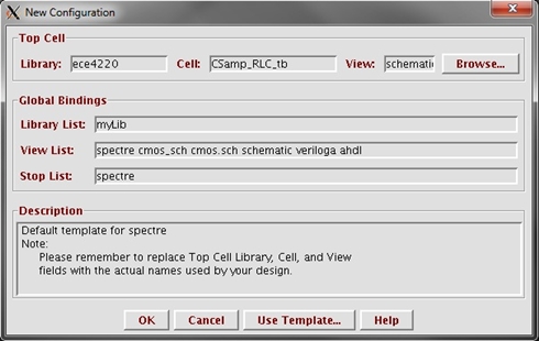
- In the New Configuration window, browse and select the schematic view. Then click the "Use Template..." button and select "spectre" in the new window. Select OK.
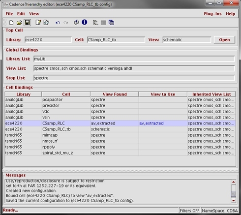
- The hierarchy editor will populate with cell bindings from the top cell. Select the appropriate cell (your circuit level, not the testbench) and enter "av_extracted" into the "View to Use" box. Save your design using the floppy disk symbol in the top toolbar and close the window.
- Now go to your testbench schematic and start the Analog Design Environment. Change the "View Name" to config either through Setup → Design... or by pressing the emitter follower symbol on the right toolbar (at the top). You may need to reload your state.
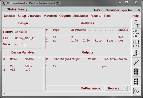
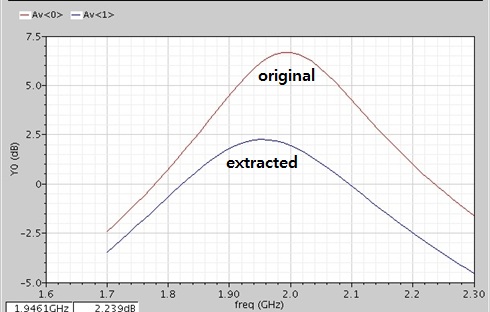
- Now run your simulation and compare the layout to the circuit (use the "Append" feature for the plotting mode and run the simulation each view).
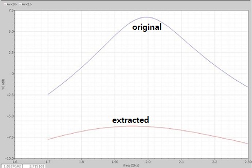
You might get a very poor result (shown below). You will need to fix your layout to reduce parasitic values.
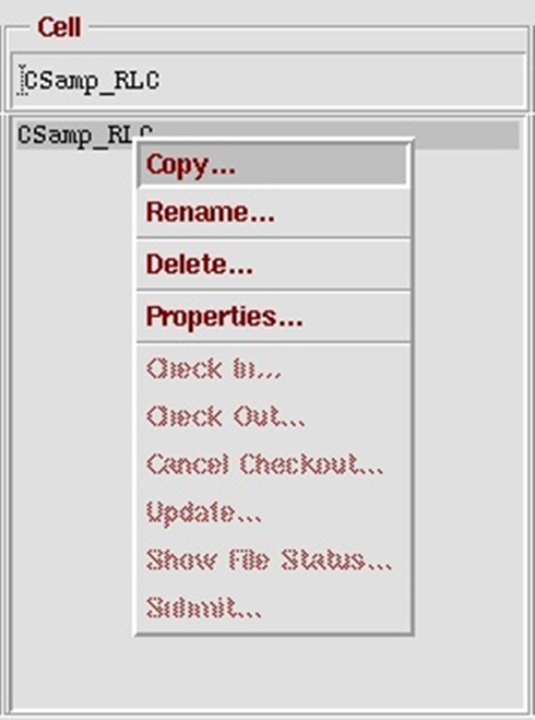
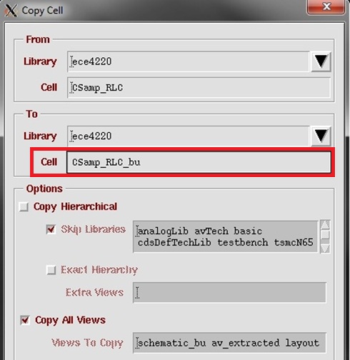
- If you need to fix your layout, do so. Remeber to run RCX again so that the av_extracted view contains the new design. Overwrite the av_extracted view so that it is automatically updated. If you want to keep a previous design, the easiest thing to do is to save the cell as a backup:
- Re-simulate with the "config" view. As you can see, increasing the line size and improving the routing can help out the design. This layout still needs some work (large lines have a lot of capacitance and there is still a fair amount of resistance added), but it is nearly there.

MICS IAP Members


