

Layout Preparation
Authors: Michael Cunningham, Ji Hoon Hyun, Dr. Dong S. Ha
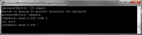
Starting Cadence
- Login to the CVL.
- Change your directory to the appropriate location (the figure below is for the ECE4220 project directory).
- Set up the environment and launch Cadence; i.e. Cadence, icfb &
Duplicate/Create a New Schematic
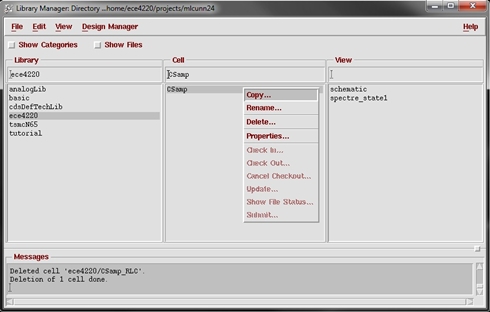
1. Open the library manager, Tools → Library Manager.... If you have already completed the previous tutorials, then simply highlight the cell we created for the AC simulation ("CSamp") and select Edit → Copy... (or right/middle click and select copy). Otherwise, you will need to create a cell (File → New → Cell View...) as is explained in the tutorial Environment Setup, in the section titled "Create a Cell View/ Schematic". The details of the schematic are covered in the next section.
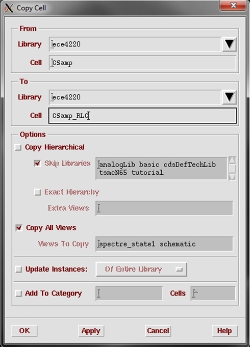
2. In the "Copy Cell" form changed the "Cell" name in the "To" section to a new name (e.g. "CSamp_RLC"). Select OK.
Editing the Schematic for Layout
- Open the new schematic cell view (CSamp_RLC). You should see the schematic you've already created.
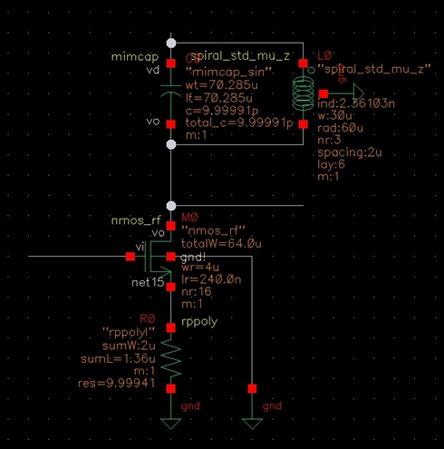
- Now, we will adjust this circuit as shown in Figure 5. The full table of all components has also been provided (make sure each of the values match up). If you need to edit an instance after placement, select the device and use the bindkey "q" to edit the object properties. Delete all unused components/net names.
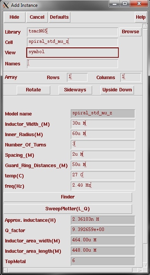
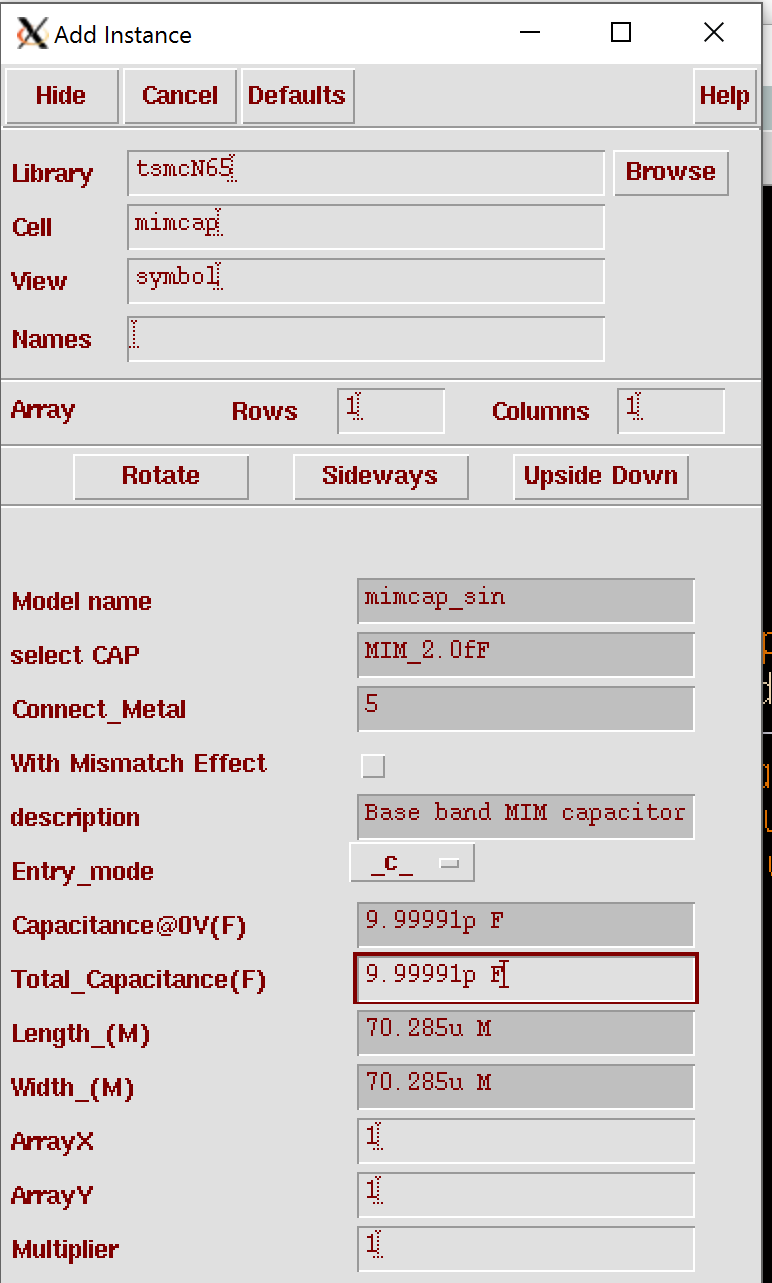
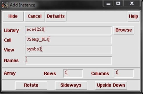
As a refresher, the figure below shows the "Add Instance" form (press "i" to add an instance).
Note that when adding the capacitor, choose “_c_” in the Entry_mode.
| Component | Description | Instance Library | Instance Cell | Parameters |
| gnd | ground | analogLib | gnd | - |
| R0 | P+ poly resistor | tsmcN65 | rrpoly | r = 10 |
| M0 | nmos | tsmcN65 | nmos_rf | wr = 4u (width) lr = 240n (length) nr = 16 (# of fingers) m = 1 (multiplier) |
| C0 | capacitor | tsmcN65 | mimcap | c = 10p |
| L0 | inductor | tsmcN65 | spiral_std_mu_z | Add the default, we will change the value in the next step. |
NOTE: Do not specify units as they are automatically appended.
NOTE: In layout, we do not fabricate off chip components/sources, so they are removed.
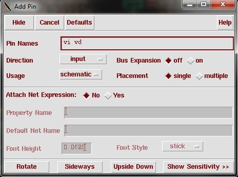
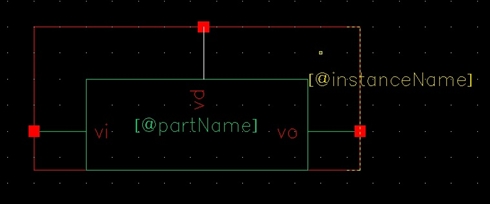
3. We must add pins to this circuit. To add a pin press "p" or select the pin button on the side bar.
4. In the "Add Pin" box, type "vi vd" with an input direction and No attached net expression.
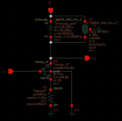
5. Place these pins at the appropriate locations. Repeat this procedure for the output pin ("vo" with an "output" direction and No attached net expression). Your schematic should look like the one below.
(Remember, you can renumber instances with Design → Renumber Instances... - I have selected X+Y+ sequencing with a 0 starting index.)
6. Now, we want to adjust the inductor value to 2.53nH for 1GHz resonance with the 10pF capacitor (ωo = 1/√LC). In order to do this we must adjust multiple parameters. Select the inductor and press "q".
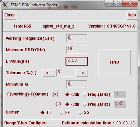
7. In the object properties editor, select the "Finder" application.
8. Enter a working frequency of "1" (GHz) and an L value of "2.53" (nH). Leave everything else as the default. Select FIND.
9. It may take a little bit of time, but when the results are displayed, you will get a window like the one below.
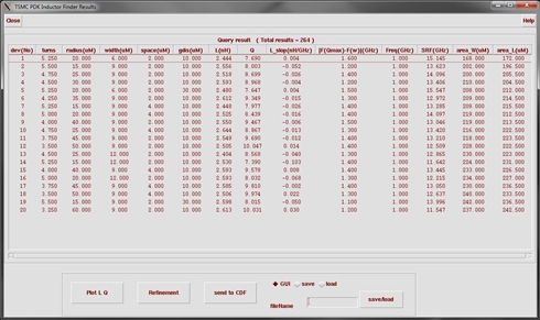
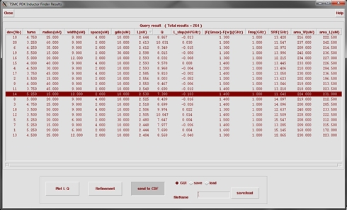
10. Select the L(nH) column to arrange the devices and select the one closest to 2.53nH. Highlight this one (device 14 for me) and select send to CDF. Close the application. I have provided the details of the inductor if you wish to enter them manually in the editor.
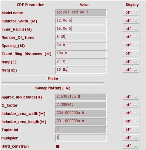
11. Once the inductor values are chosen, select OK to return to the schematic. You may need to redraw/resize the display ("F6"/"f") and you will want to check and save ("Shift + x").

FUN FACT: It is often customary to include "dummy" resistances and transistors in the pin schematic when good matching between multiple devices is required. The reason this is done has to do with fabrication - components on the edges typically receive the majority of process variation. For this reason, the dummies are inserted on the sides of the devices and are shorted (so they play no role in the design) and are tied to ground or the rail voltage. Dummy transistors can also be inserted within a long train of interdigitate transistors to create a buffer between two FETs with different drain/source voltages. This will often cause the dummy FET to have different S/D voltages, so the gate must be biased for cutoff.
Create a Symbol View
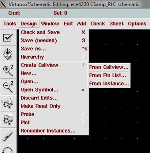
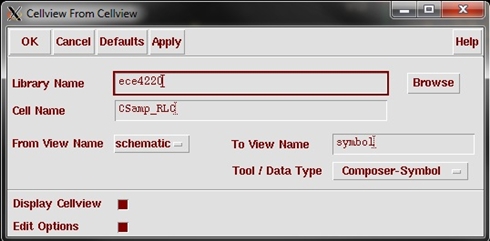
1. We need a way to test this circuit, but before we can set up a testbench we need to create a symbol that represents this circuit. Go to Design → Create Cellview → From Cellview.... In the new window, make sure that it is from "schematic" to "symbol" with data type "Composer-Symbol". Select OK.
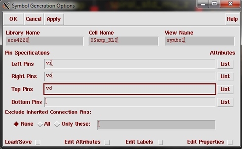
2. In the next window, select what side of the symbol you want your pins to be on. I've arranged the pins as shown below. Select OK.
3. A new cell view will open with the symbol you just created. Save ("Shift + s") and close the window.
Create a Testbench
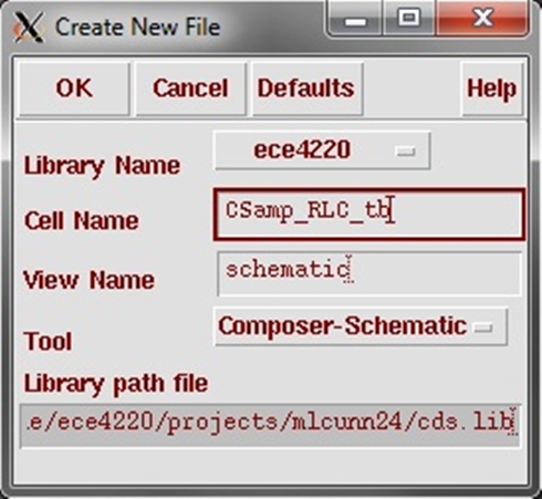
1. Create a new cell view from the schematic window Design → New..., or from the library manger/icfb window. Give it a relevant name (e.g. "CSamp_RLC_tb"). Make sure it is a schematic and selectOK. If you create the cell from the schematic window, it will close the opened design and open the new one.
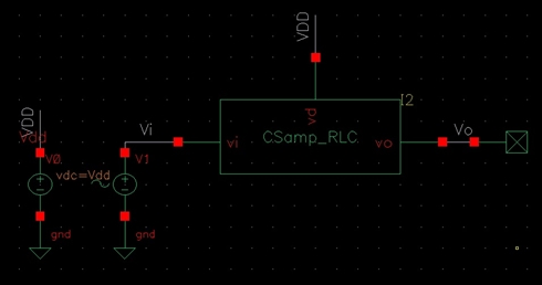
2. Save the cell view and then add an instance ("i"). Select your library name, cell, and the symbol view (that we just made). Place it on the schematic.
3. Next, add the bias circuitry and labels as shown in the table and figure below.
| Component | Description | Instance Library | Instance Cell | Parameters |
| V0 | ac voltage source | analogLib | vsin | AC magnitude = 1m DC voltage = Vg |
| V1 | dc voltage source | analogLib | vdc | DC voltage = Vdd |
| gnd | ground | analogLib | gnd | - |
| - | no connection | basic | noConn | - |
NOTE: You can descend the hierarchy of a selected instance by using the bindkey "e" to read or "Shift + e" to edit. To ascend, press "Ctrl + e".
4. Check and save ("Shift + x") and then open the analog design environment ("ADE") by Tools → Analog Environment.
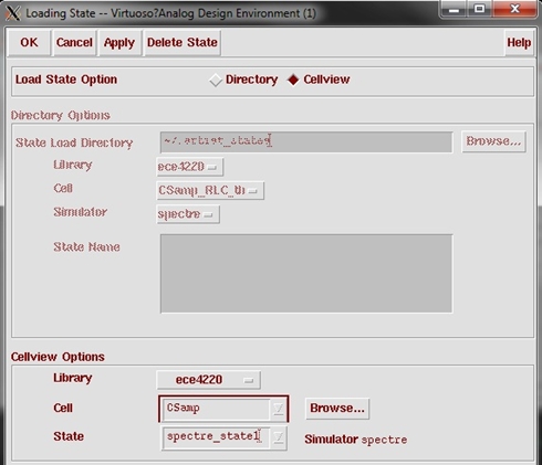
5. In the ADE, go to Session → Load State. Select Cellview and from the drop-down menu, select CSamp (from the first tutorial). If you did not set up a state, please see the AC Simulation tutorial for instructions on how to do this.
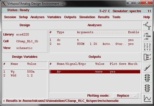
6. The state should load. Delete any unused design variables (we only need Vg and Vdd - see values in Figure 23). To delete, double click on the variable and select delete, or highlight the variable and choose Variables → Delete.
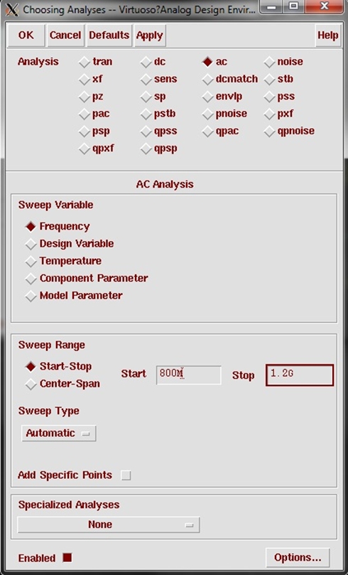
7. Adjust the "ac" sweep frequency from "800M" to "1.2G". Select OK.
8. Your outputs should already be setup from the AC Simulation tutorial.
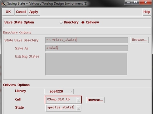
9. Now save this state to the testbench cell. Session → Save State, select Cellview and verify that the correct cell is listed. Select OK.
NOTE: When saving a state, make sure all plots are closed or they will be saved as part of the state (and are reopened when loading that state).
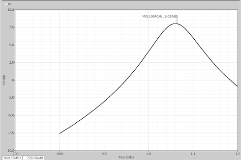
10. To verify that you set up everything correctly, run the simulation by pressing the green traffic arrow icon (make sure you have checked and saved). We can see a graph that resembles Figure 25 below.
NOTE: You may get a peak at different frequency and different gain values depending on your inductor, e.g., ~5.3dB gain peaking at 1GHz.

MICS IAP Members


