

DC Simulation
In this tutorial, you will learn how to run DC simulation and find parameters for an NMOS.
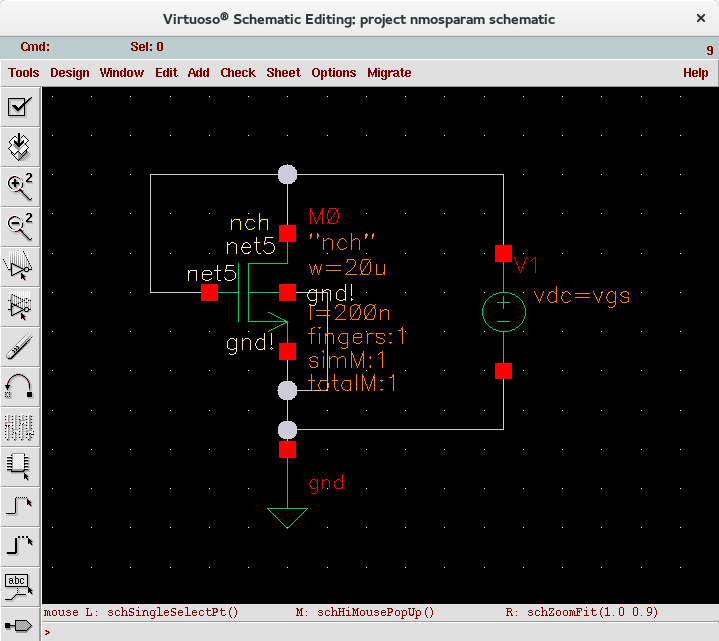
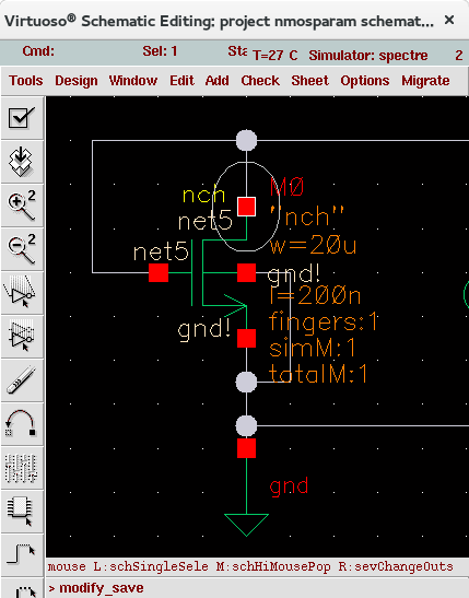
1. Create a schematic as shown in the figure. Include an NMOS (nch) from the technology library, and voltage source (vdc) and ground (gnd) from analogLib. Change the W/L of the NMOS to 20µm/200nm. Connect drain and gate of NMOS together to ensure saturation mode, and ground the NMOS bulk. Set the DC voltage as a parameter “vgs”.
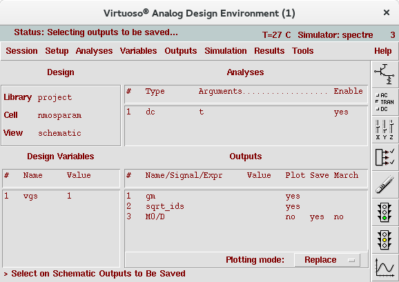
2. Start Analog Design Environment (ADE) from Tools à Analog Environment. You will get to a similar window as below but without the items listed under “Design Variables”, “Analyses”, and “Outputs” section. We will add the items with the following steps.
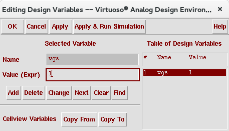
3. In ADE window, go to Variables à Copy From Cellview. The parameter “vgs” will appear under “Design Variables”. Double click on “vgs” or click on “Edit Variables” button on the right, set “vgs” to 1 and click the Change button. This is just a nominal value since we will sweep its value. Click OK to close the window.
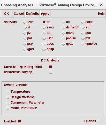
4. In ADE window, go to Analyses à Choose, or click the “Choose Analyses” button on the right. Click on “dc” and select “Save DC Operating Point”. DC simulation is now enabled. Click OK to close the window
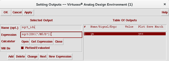
5. In ADE window, go to Outputs à Setup, or click the “Setup Outputs” button on the right. Put the name as “gm”. Click on the “Open” button to open the calculator. Click on the dc tab and select idc, then go to the schematic and click on the drain node of the NMOS. Go back to the calculator and select “deriv” from the list of functions. Now go back to “Setting Outputs” window and click on “Get Expression” button, then click “Add” button to add it to output.
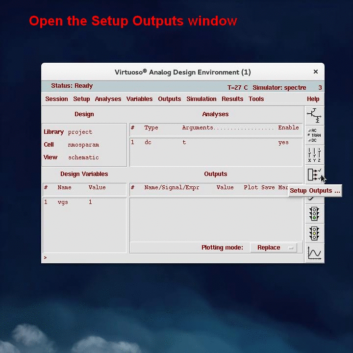
Figure 5. Setup output for gm.
6. Repeat the above procedure to setup an output for the square root of IDS, “sqrt_ids”. If you know the function, you can just type into the expression field.
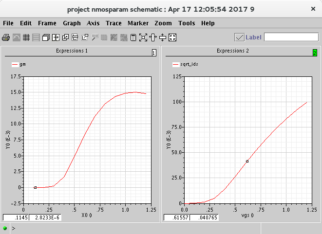
7. From ADE window, go to Outputs à To Be Saved à Select On Schematic, then select the drain node of the NMOS. This will enable the drain current for the calculations set in steps 5 and 6. Next, press ESC in schematic window to exit output selection mode. In the future, you should always save the currents for all calculations
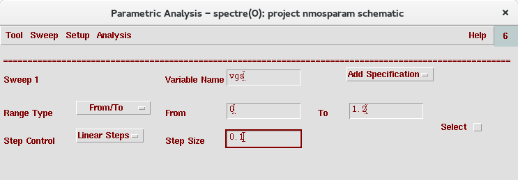
8. You now have the ADE window as shown in Figure 2. Now we’re going to do a sweep on the parameter “vgs”. Go to Tools à Parametric Analysis, set variable name as “vgs, and sweep from 0 to 1.2 with linear steps of 0.1. Go to Analysis à Start to run the sweep.
9. You will get the output plotted in a new window. You can find transconductance gm on the left, and square root of IDS on the right. You can estimate VTH and µnCox from the plot of square root of IDS. The slope of the curve is (0.5µnCoxW/L)^0.5.
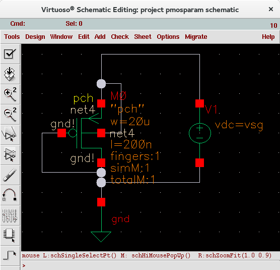
10. You can do the same to a PMOS. Create a schematic as below for example, and repeat steps 2 through 9. Note that you should use the absolute value of drain current since the square root calculator will not be able to process negative values.
11. To find ro values, create a schematic with separate vgs and vds parameters.
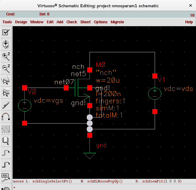
12. Similar to step 3, set nominal values for vgs and vds as 1.
13. Similar to step 4, from the Choose Analyses window, enable “Save DC Operating Point” of dc analysis.
14. Similar to step 7, save the drain current of the NMOS.
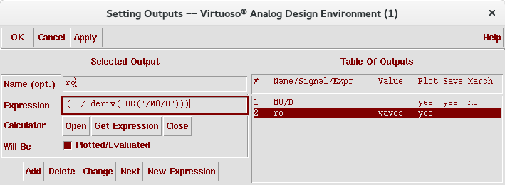
15. In the “Setting Outputs” window, create an output “ro” by performing derivative of IDS versus VDS with the expression “1/deriv(IDC(“/M0/D”))”. Make sure the current refers to the NMOS in your schematic.
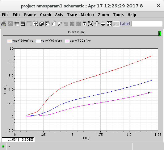
16. Setup parametric analysis as shown below. The sequence is important. Make sure that vgs is the first variable while vds is the second. This will generate three curves of IDS vs VDS in regard to three VGS values.
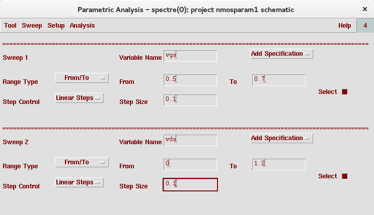
17. Run simulation by going to Analysis à Start. You will get values of ro values with respect to bias condition.

MICS IAP Members


