

Introduction to Cadence for Analog IC Design
In these tutorials you will be working with TSMC 65nm process design kit (PDK), available through MOSIS. The information contained in the design kit is extremely confidential and you are recommended to consult your course instructor before disclosing any results obtained in your class project/assignments. This is a short tutorial meant to assimilate those who are new to Cadence Design Environment. In order to use Cadence software you will need an account in CAD and Visualization Lab (CVL).
Circuit Level Simulation
- Creating Libraries and Schemantics in Cadence: create a library that is attached to TSMC 65nm CMOS library, and the basic steps to create simple a schematic.
- DC Simulation: Learn how to run DC simulation and find parameters for an NMOS.
- AC Simulation - 1: Setup a schematic for AC simulation
- AC Simulation - 2: Setup an AC simulation and outputs
- List of bindkeys for Cadence 5.1.41.
Layout and Post Layout Simulation
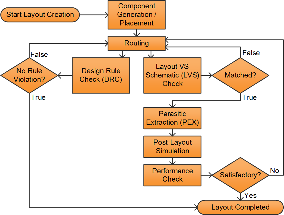
A typical process for working on layout is shown in the graph above. Layout is completed when DRC shows no violation and performance of post-layout simulation is satisfactory. Each step is described in detail in pages below.
- Start Layout: Create a pin schematic, symbol view, and testbench in preparation for layout.
- Component Placement: Identify components and place them at appropriate location.
- Routing: Connecting components.
- Design Rule Check: Check if layout obeys design rules.
- Layout VS Schematic: Check layout components are correctly connected.
- Parasitic Extraction and Post-Layout Simulation: Extracting parasitics with Assura and include it into simulation.
Troubleshooting and Customization
- Troubleshooting: Troubleshoot possible errors that may arise.
- Environment Customization: Set personal preferences in Cadence.
Miscellaneous
- Backup of Placement and Routing: Basic idea of component placement and routing.
- TSMC Dummy Layer Auto-fill: (Not yet available) Learn the procedure to use the automatically generated dummy layer fill for density DRC rules in layout.
Comments to: ha@vt.edu

MICS IAP Members


