

How to Solve DRC Errors
Authors: Michael Cunningham, Joseph Chong, and Dr. Dong S. Ha
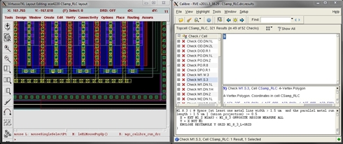
DRC Debugging
1. Go to the RVE window. Here, there is a list of errors and a description in the bottom box. We will only focus on/disregard the following as mentioned:
a. All "CSR.*" (Corner Stress Relief) errors can be ignored. Metals and vias are not allowed in chip corners, but we are not creating the entire chip.
b. Any "*.EN" (Enclosure) errors regarding chip edge can be waived; all others should be resolved according to the rule described in the explanation window.
c. All "*.S" (Spacing) errors should be resolved. Move metals or vias to meet the minimum spacing requirements.
d. All "*.W" (Width) errors should be resolved. Resize any flagged objects to meet the maximum/minimum width rules.
e. All "*.A" (Area) errors should be resolved. Resize the metal/via as described in the check.
f. All "G.*" (Grid) errors should be resolved. The grid is the minimum resolution that can be manufactured. If you used paths with variable ends and specified a length less than the grid resolution (for some unknown reason), you will receive an error. All other path ends are fixed to the grid.
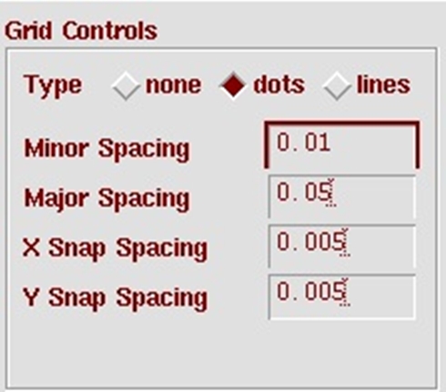
Additionally, do not change the grid resolution from 0.005 in the layout display options ("e").
g. All "IND.DN" (Inductor Density) errors can be waived as this is one segment of a chip. This error is generated if the inductor is too large compared to the chip.
h. All ".DN" (Density) errors should be resolved (with the exception of the aforementioned case). Certain metal and oxide densities are required for fabrication. TSMC recommends their autofill script, but I will not cover this as it is better suited for those with sufficient layout experience.
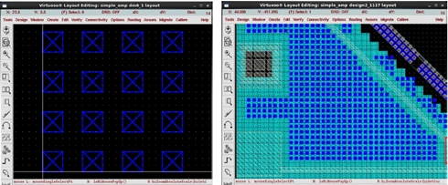
Alternatively, you can satisfy this error by manually adding in dummy layers of metal - Mx(dm) - thin oxide for device - OD(dm) - and polysilicon oxide - PO(dm) in the empty areas of your chip. This image below is a 4 x 4 array of dummy layers OD, PO, M1, M2, M3, M4, M5, and M6 vertically aligned. Each square is 3μm x 3μm with 3μm spacing.
2. Once you select a check/cell in the left column, double-clicking or pressing the light button in the toolbar will highlight and zoom in on the error. Follow the description to resolve the error.

MICS IAP Members


