Nonlinear Simulation for an Amplifier
P1dB and IIP3 Simulation for Amplifiers
Authors: Joseph Chong, Ji Hoon Hyun, and Dr. Dong S. Ha
In this section you will learn how to run P1dB and IIP3 simulation for an RF amplifier working at 2.4G. Check out this workshop tutorial for more information.
Create Schematic
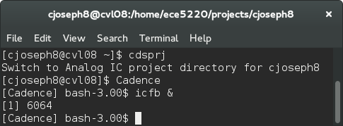
1. Start Cadence Virtuoso under the folder with cds.lib linked to TSMC library, i.e., run “cdsprj” to change to folder, then run “Cadence” and “icfb &”.
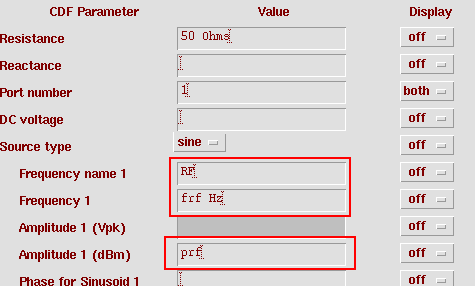
2. Create a new schematic by File->New->Cellview under icfb window. Make sure the library is the one attached to TSMC library (e.g., ece5220). Insert instances and connect them together as shown in Fig. 2 below. Note that we need to set extra parameters in PORT0 shown in the figure. After completed the schematic, check and save.
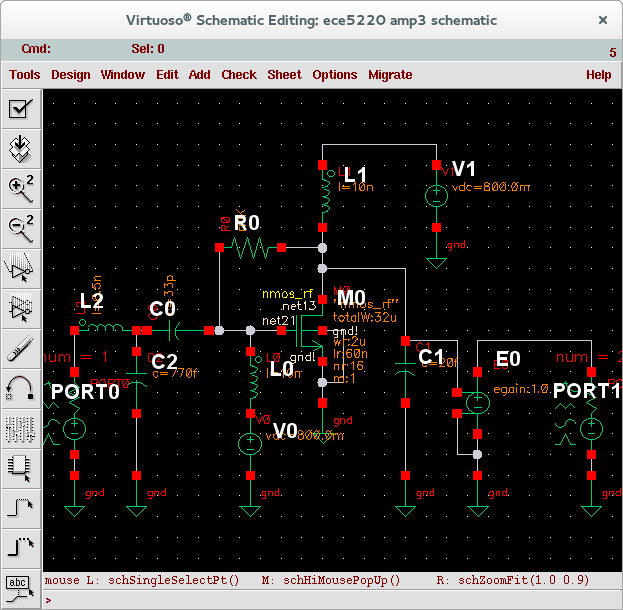
| Component | Description | Instance Library | Instance Cell | Parameter |
| V0, V1 | Voltage Source | analogLib | vdc | DC = 0.8 |
| PORT0 | Port | analogLib | port | Resistance = 50 / Port number = 1 / Source type = sine / Freq name 1 = RF / Frequency 1 = frf / Amp 1 (dBm) = prf |
| PORT1 | Port | analogLib | port | Resistance = 50 / Port number = 2 |
| L0 | Inductor | analogLib | ind | L = 10n H |
| L1 | Inductor | analogLib | ind | L = 10n H |
| L2 | Inductor | analogLib | ind | L = 6.5n H |
| C0 | Capacitor | analogLib | cap | C = 33p F |
| C1 | Capacitor | analogLib | cap | C = 20f F |
| C2 | Capacitor | analogLib | cap | C = 770f F |
| E0 | Buffer | analogLib | vcvs | Gain = 1 |
| R0 | Resistor | analogLib | res | R = 1k |
| M0 | Transistor | tsmcN65 | nmos_rf | wr = 2u / lr = 60n / nr = 16 |
P1dB Simulation
3. After completed the schematic, click Check and Save button. Then start Analog Design Environment from Tools -> Analog Environment. Select Variables->Copy from Cellview to get the variables prf and frf shown in Design Variables section. Set prf = -30 and frf = 2.4G.
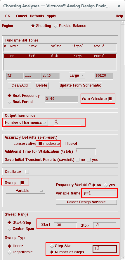
4. Go to Choosing Analyses window and select pss simulation. Select Auto Calculate for automatic calculation of beat frequency. In the Output Harmonics field, set the cyclic to Number of harmonics and set the number of harmonics to 3. In the Accuracy Defaults field, select the moderate button. Click on the Sweep button, set Variable Name to prf, Sweep Range to -30 to -5, Sweep Type to Linear and Number of Steps = 10. Your Choosing Analyses window should look like below.
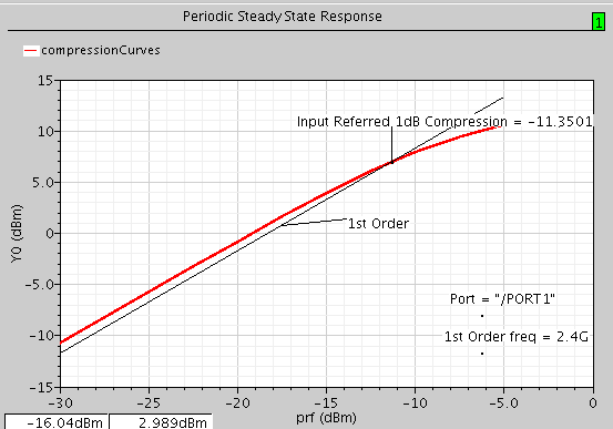
5. Click Netlist and Run icon (green traffic light). After simulation completed, go to Results->Direct Plot->Main Form. In the Direct Plot Form, click on Compression Point and 2.4G in the 1st Order Harmoniclist. Click on PORT1 (the output port) on schematic to plot P1dB.
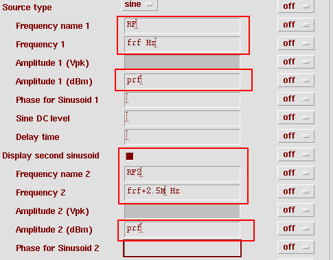
6. Back to the schematic, edit the properties of instance PORT0 to add a frequency RF2. Click on Display second sinusoid button, the set Freq name 2 = RF2, Freq 2 = frf + 2.5M, Amp 2 = prf. Check and save.
IIP3 Simulation
7. Back to the schematic, edit the properties of instance PORT0 to add a frequency RF2. Click on Display second sinusoid button, the set Freq name 2 = RF2, Freq 2 = frf + 2.5M, Amp 2 = prf. Check and save.
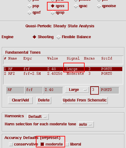
8. Go to Choosing Analyses window, disable all other simulations, and select qpss simulation. Set RF Signal as Large. In the Accuracy Defaults field, select moderate. Your Choosing Analyses window should look like below.
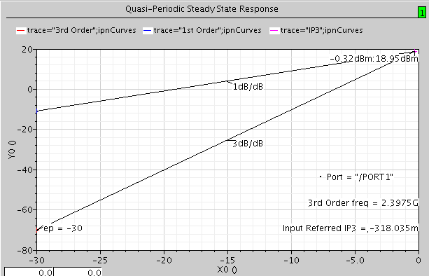
9. After simulation is completed, choose Results->Direct Plot->Main Form. Select the qpss button and IPN Curves button. Set Single Point Input Power Value (dBm) = -30. Select 2.398G in 3rd Order Harmonic and 2.402G in 1st Order Harmonic. Click on PORT1 (the output port) on schematic to plot IIP3.
