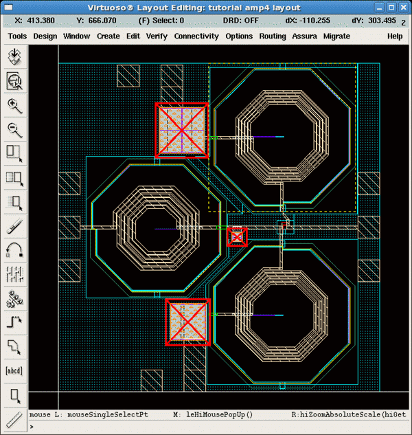
Layout of an Amplifier
Authors: Joseph Chong, Ji Hoon Hyun, and Dr. Dong S. Ha
In this section you will learn how to create layout of an amplifier. You need to split your schematic into two parts: the on-chip components part, and the off-chip components part. After the schematics are created, we will draw a chip layout for the on-chip components.
Creating On-chip Components Schematic
1. Create a core amplifier schematic as shown in figure below. Insert pins with the button on the left panel. Name the four pins according to what is shown in the figure.
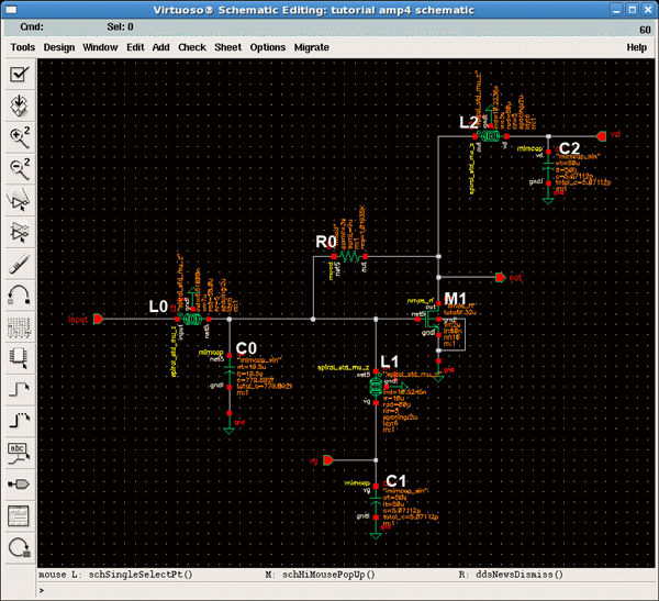
| Component | Description | Instance Library | Instance Cell | Parameter |
| L0 | Inductor | tsmcN65 | spiral_std_mu_z | w=7u / r=47u / turns=5.5 |
| L1, L2 | Inductor | tsmcN65 | spiral_std_mu_z | w=5u / r=70u / turns=5.25 |
| C0 | Capacitor | tsmcN65 | mimcap | l=19.5u / w=19.5u |
| C1 | Capacitor | tsmcN65 | mimcap | l=80u / w=80u |
| C2 | Capacitor | tsmcN65 | mimcap | l=80u / w=80u / ArrayX = 2 / ArrayY = 2 |
| R0 | Resistor | tsmcN65 | rnwod | w=3u / l=9u |
| M1 | Transistor | tsmcN65 | nmos_rf | wr = 2u / lr = 60n / nr = 16 |
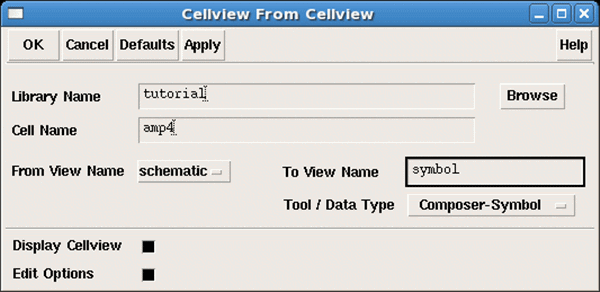
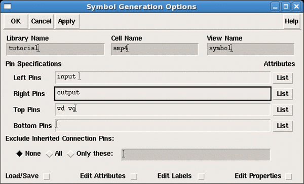
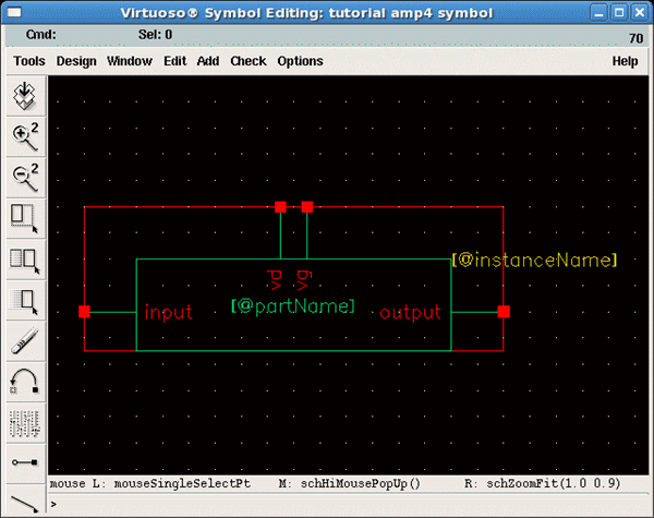
2. Create a symbol cellview. Go to Design->Create Cellview->From Cellview. At the first window, make sure it is from schematic to symbol, click OK. At the second window, you can arrange the placement of the pins as you like. Let's place vd and vg on top. Click OK. You will then get a schematic window displaying your symbol. Save and close.
Creating Off-chip Components Schematic (Testbench)
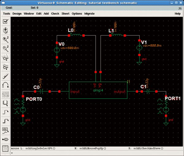
3. Create a new schematic as testbench shown in figure below. We will place all the off-chip components in testbench schematic. These components are for simulation purpose and will not appear in our layout. You can start Analog Design Environment and run some simulations on the circuit if you like.
| Component | Description | Instance Library | Instance Cell | Parameter |
| V0, V1 | Voltage Source | analogLib | vdc | DC = 0.8 |
| PORT0 | Port | analogLib | port | Resistance = 50 / Port number = 1 |
| PORT1 | Port | analogLib | port | Resistance = 50 / Port number = 2 |
| L0, L1 | DC Feeding Inductor | analogLib | ind | L = 100n H |
| C0, C1 | DC Blocking Capacitor | analogLib | cap | C = 33p F |
Generating Components in Layout
4. Go back to the core amplifier schematic. On the top menu, select Tools->Design Synthesis->Layout XL and Create New layout cellview. You will get an empty layout editor view.

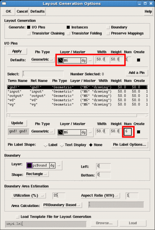
5. From the layout editor menu, select Design->Gen from source .... A layout generation option windows appeared and prompts users to setup the pin layers, pin width, pin height, boundary layer ... and so on for layout generation. You may have a predefined size that you want to create a boundary for your layout in the future, but for now, deselect the Boundary button under Layout Generation category. Then, under I/O Pins section, select M6 / dg for Layer / Master and set Width and Height to 50. Click Apply button. This will create the pins on Metal layer 6 (top layer). Next, select "gnd!" pin in the list, then set Num field to 6 to create six GND pins. Click Update. Your window will look as shown below. Click OK when done.
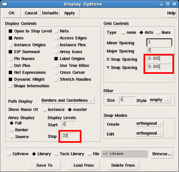
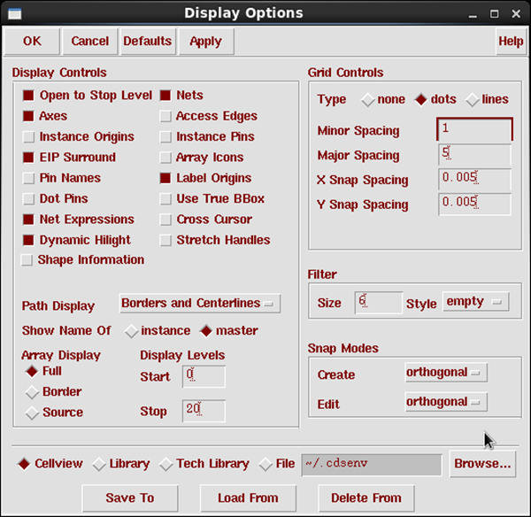
6. Back to layout editor window. You may want to select Edit->Place As In Schematic for an initial placement. The unit in layout editor is 1um. We need to get the snap grid to match our layout resolution so that shapes from library will not be off-grid in our layout. Go to Options->Display and change X/Y Snap Spacing to 0.005. Change Display Levels stop level to 20 so that we can see into the hierarchy of library instances. The Display Options window will look as shown below.
Full Custom Layout
We now use Virtuoso Layout Editor for a full custom layout. Full custom in RFIC area usually means manual drawing of interconnection between components. The reason is that computer automation do not quite know how to handle transmission lines, electromagnetic coupling interference, etc., which are the important factors for good RF performance. One knows how to draw a layout optimized for these performance factors mainly through experience.
In some special occasions, one would need to draw a transistor manually. But in most circumstances, the MOSFET from process design kit (PDK) library is directly used. Resistors, inductors and capacitors are also directly from library. Therefore, only the floorplanning and metal connection are discussed in this tutorial.
I. Floorplanning.
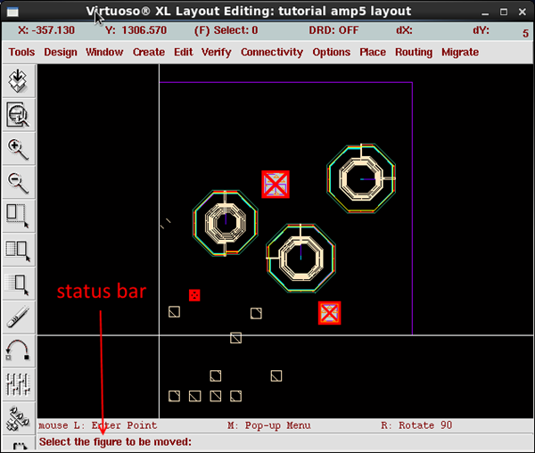
a. Moving: Press key "m" to start MOVE function. The status bar will tell you which function is currently enabled. To end MOVE function, press ESC. You can view the connections between components by enabling "Nets" in the menu Options->Display.
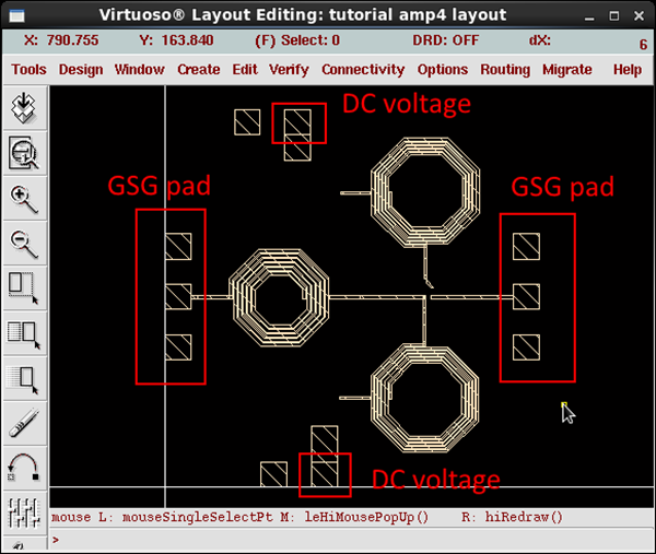
b. I/O pads: Usually RF input and output pads are arranged in Ground-Signal-Ground sequence (single ended) or G-S-S-G sequence (differential). This will provide a 50 ohms characteristic impedance interconnect.
The size of a RF probe is very large comparing to a chip, therefore only one group of RF I/O pad can be placed on each side of the chip. I assume that the probe is G-S-G with pitch-to-pitch distance of 100um. Input pad and output pad is placed at the left and right side, respectively.
See Microwaves101's page for photo of probe station and probes.
c. Active Devices: I personally suggest placing active devices or resistors together when it is convenient. The reason for this, is that interconnection between distant component are usually done with Microstrip lines on Metal 6, and it is troublesome to go from Metal 6 to the active components. (This will be explained later)
II. Interconnect
a. Rectangles: Since this is a full-custom layout, we create all interconnect by drawing rectangles. Press "r" key to start creating rectangles. You may also want to explore the different shapes under "Create" menu, and also the shape editing functions including stretch and merge under "Edit" menu.
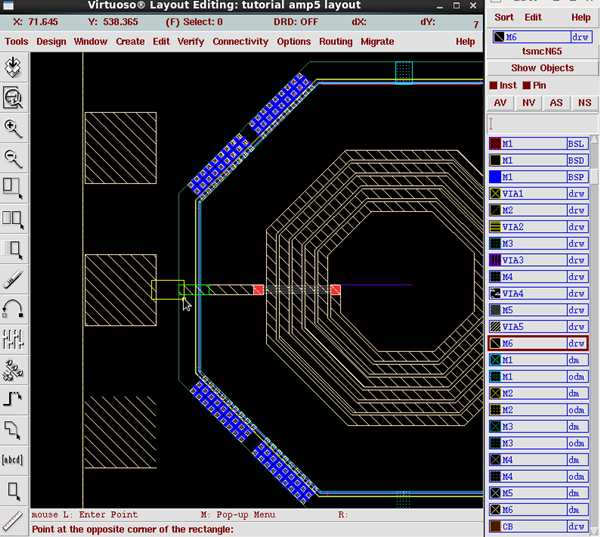
b. Transmission lines: RF signal interconnect are done with transmission lines. The most commonly used transmission lines are Microstrips and Coplanar Waveguides. To create a microstrip, draw the signal rectangles on the top M6"drw" layer and ground plane on bottom M1"drw" layer.
The technology that we're currently using has thickness of M6 as 3.4um, the height between M6 and M1 is 3um. With the relative permittivity oxide is around 4, a good rule of thumb is the width should be twice the height, which is width of 6um.
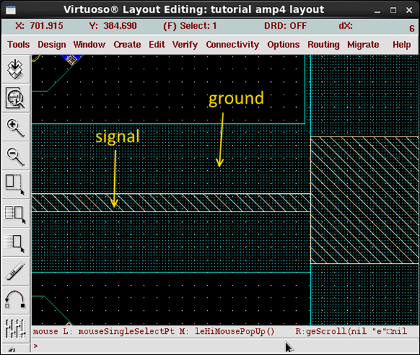
For more details, please take a look at the design document, under "interconnect" section. The document is located on CVL at
/home/ece5220/TN65CMSP018_1_1.pdf
Please note that this is a confidential document. You have signed an agreement not to distribute it.
c. Vias: We can see that the signal line at M6 is directly connected to a pad on M6 layer. The ground plane on M1 should also be connected to the GND pad at M6 layer. In order to achieve this, we should go layer by layer.
First, we want to connect M1 to M2. We start by drawing a rectangle on layer VIA1"drw", overlap with M1. This means we have a vertical via connecting M1. Then we draw a rectangle on layer M2"drw", overlap with VIA1. By this we have a connection from M1 to M2.
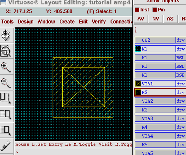
We will need to continue this procedure until we reach M6. Therefore a rectangle on each of VIA2"drw", M3"drw", VIA3"drw", M4"drw", VIA4"drw", M5"drw", and VIA5"drw" layers. By doing this we connect M6 with M1. Actually there are design rules for the size of rectangles on VIA layers and also its distance between the edge of metals. But for now let us ignore them.
You can do this connection for once, and then copy this whenever your want a vertical connection.
d. MOSFET connection: A MOSFET in this PDK comes with 4 pins: gate, drain, source, and bulk. If you enable "Pin Names" from "Options->Display" menus, you can see that each pins are to be connected at different metal layers. Gate at M3, drain at M2, source at M4, and bulk at M1.
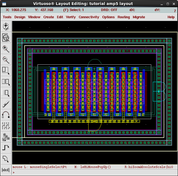
To connect to the gate of MOSFET from a transmission line at M6, just go through the same procedure describe in the previous section.
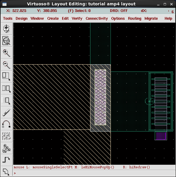
e. DC connections: Voltage source is AC short in simulation, but actually they're not. Larger capacitors on chip is to create a AC short path for RF signals. Connections to these capacitors should be as short as possible.
If you must route a trace for DC voltage and current, a good rule of thumb is that you need at least 1um of trace width for 1mA of current. These traces can be routed on layers other than M6.
Final Layout
