

Back End Design Using Cadence Tool – Physical Implementation
Authors: Hetaswi Vankani, Adithya Venkatramanan, and Dr. Dong S. Ha
Tool: Encounter Digital Implementation (encounter)
Input Data
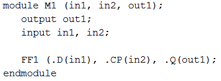
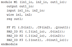
1. Synthesized netlist, IO pad insertion
The synthesized, IO pad inserted netlist can be downloaded from here: cnt_updown_dve.v
Explanation of the changes made:
In order to insert the pad an input signal to the pad and an output signal from the pad is required. For an input pad, the input signals are the external signals being applied to the module whereas the output signals are the signals (wires declared in Verilog) being used by the various gates in the module. In case of an output pad, the input signals are the modules internal signals whereas the output signals are the output signals of the module.
The library (tpdn65gpgv2od3_sdbc.lib) must be checked for appropriate cells for IO pads. These are then instantiated. The synthesized file from generated from the synthesis stage does not have the pads instantiated by default. In order to do so, all signals going into the module can be assumed as the internal signals. Thus, in module declaration statement additional prefix/suffix must be added to the signals to tell them apart from the signals input/output to pad and those input/output to the module.
- viewDefinition.view
This file is generally set for multi-mode multi corner analysis. But, for the purpose of this tutorial, only one view has been considered.
The file viewDefinition.view can be downloaded from here: viewDefinition.view - Timing constraint file
Having changed the synthesis file ‘cnt_updown_dve.v’ even, the sdc file constraints need to be renamed. The modified sdc file can be downloaded from here: cnt_updown_syn.sdc - Clock specification file
This file can be downloaded from here: Clock.ctstch - Path to timing library, LEF files - theses paths may be required during import design stage.
Common timing library:
/software/PDK/65nm_TSMC/Mosis_Doc/65nmLibs/tcbn65gplus/tcbn65gplus_frontendzipped/tcbn65gplus_140b_nldm/
TSMCHOME/digital/Front_End/timing_power_noise/NLDM/tcbn65gplus_140b/tcbn65gplusbc0d88.lib
/software/PDK/65nm_TSMC/Mosis_Doc/65nmLibs/tpdn65gpgv2od3_sd/tpdn65gpgv2od3_sd/tpdn65gpgv2od3_sd_200a_nldm/
TSMCHOME/digital/Front_End/timing_power_noise/NLDM/tpdn65gpgv2od3_sd_200a/tpdn65gpgv2od3_sdbc.lib
LEF files:
/software/PDK/65nm_TSMC/Mosis_Doc/65nmLibs/tpdn65gpgv2od3_sd/tpdn65gpgv2od3_sd/tpdn65gpgv2od3_sd_200a_sefu6lm/
TSMCHOME/digital/Back_End/lef/tpdn65gpgv2od3_sd_200a/mt_2/6lm/lef/tpdn65gpgv2od3_sd_6lm.lef
/software/PDK/65nm_TSMC/Mosis_Doc/65nmLibs/tpdn65gpgv2od3_sd/tpdn65gpgv2od3_sd/tpdn65gpgv2od3_sd_200a_sefu6lm/
TSMCHOME/digital/Back_End/lef/tpdn65gpgv2od3_sd_200a/mt_2/6lm/lef/antenna_6lm.lef
/software/PDK/65nm_TSMC/Mosis_Doc/65nmLibs/tcbn65gplus/tcbn65gplus_backendzipped/tcbn65gplus_200a_sef/
TSMCHOME/digital/Back_End/lef/tcbn65gplus_200a/lef/tcbn65gplus_6lmT1.lef
Capacitance table:
/software/PDK/65nm_TSMC/Mosis_Doc/65nmLibs/tcbn65gplus/tcbn65gplus_backendzipped/tcbn65gplus_200a_sef/
TSMCHOME/digital/Back_End/lef/tcbn65gplus_200a/techfiles/captable/cln65g+_1p06m+alrdl_typical_top1.captable
qrcTech file:
/software/PDK/65nm_TSMC/Mosis_Doc/65nm_general_purpose_logic_CLN65GP/T-N65-CL-SP-031-V4/T-N65-CL-SP-031-V4_12a/RC_QRC_cln65g+_1p6m_4X1Z_alrdl_5corners_12a/RC_QRC_cln65g+_1p06m+alrdl_typical/qrcTechFile
Comments to: ha@vt.edu

MICS IAP Members


