

Creating Schematics in Cadence
Authors: Michael Cunningham, Ji Hoon Hyun, Dr. Dong S. Ha
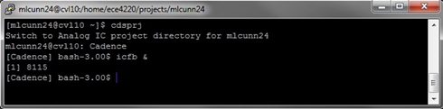
Starting Cadence
- Login to the CVL.
- Change your directory to the appropriate location (the figure below is for the ECE 4220 project directory).
- Set up the environment and launch Cadence; i.e. Cadence, icfb &
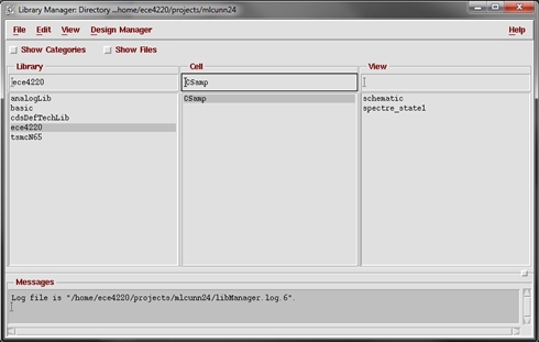
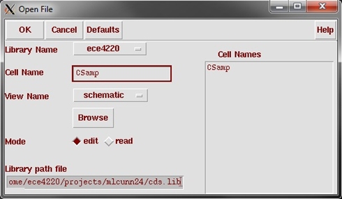
- Open your schematic by one of the methods below or create a new one as is done in the Environment Setup tutorial.
1. In the icfb window go to Tools → Library Manager... and then select the desired library and cell.
2. In the icfb window go to File → Open and then select the desired library name and cell name.
Schematics in Cadence
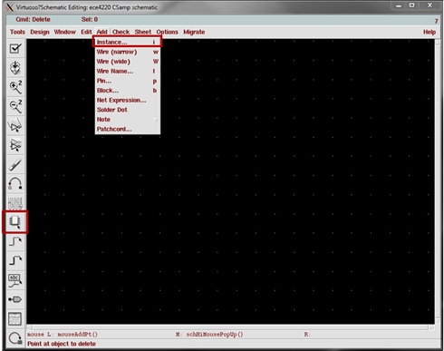
- First we will want to place the components we need to make a basic common source amplifier. In the schematic window, create a new instance by using one of the following methods:
1. Using the bindkey "i".
2. Selecting the IC icon in the icon bar.
3. Select Add → Instance from the toolbar.
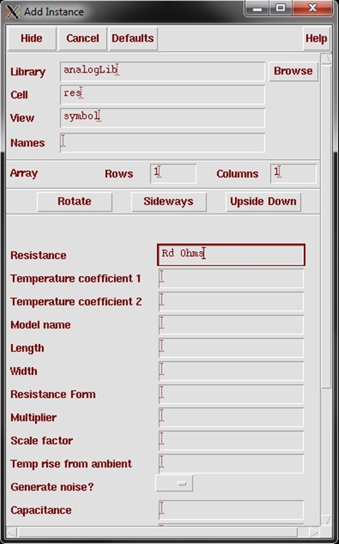
- In the Add Instance dialog box, select the symbol view for a resistor as shown below. Set the resistance to variable called "Rd". This will be our drain resistor.
- Select the schematic window. You should see the component symbol (yellow) attached to your cursor. Place the device by selecting a point on the schematic. Press "Esc" to finish placing components.
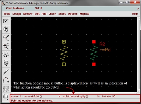
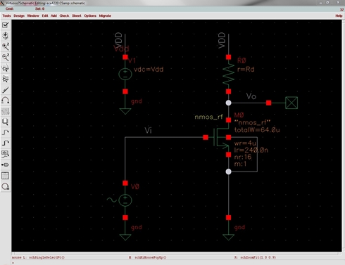
- Repeat this procedure for the rest of the devices. The table below lists all the components, their libraries, and their parameters. If you need to edit an instance after placement, select the device and use the bindkey "q" to edit the object properties. (See the schematic below for placement.)
Component Description Instance Library Instance Cell Parameters R0 resistor analogLib res r = Rd V0 ac voltage source analogLib vsin AC magnitude = 1m
DC voltage = VgV1 dc voltage source analogLib vdc DC voltage = Vdd gnd ground analogLib gnd - - no connection basic noConn - M0 nmos tsmcN65 nmos_rf wr = 4u (width)
lr = 240n (length)
nr = 16 (# of fingers)
m = 1 (multiplier)
NOTE: Do not specify units as they are automatically appended.
Below are some useful bindkeys to make placement easier.
Keystroke Function Action Esc (Escape) Cancel Current Function F3 Current Function Options Form F6 Redraw Display Delete Delete the selected component or wire c Copy instance f Zoom fit i Create Instance m Stretch (move with wires attached) Shift + m Move (selected only) q Query (object properties) r Rotate Ctrl + r Flip (vertical) Shift + r Mirror (horizontal) u Undo Shift + u Redo w Create wire Shift + x "Check and Save"
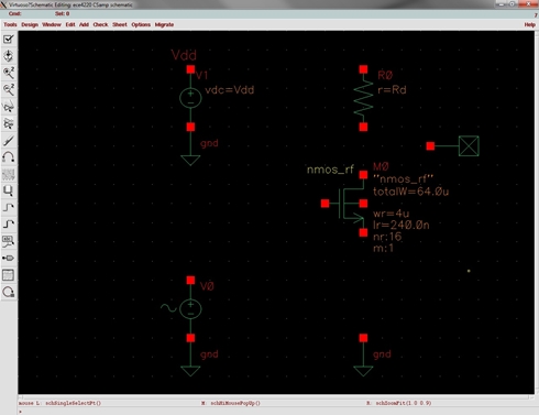
- Once you finish, you should have something that looks like the schematic below. After everything is placed, it's a good idea to renumber the instances (but not required). To do this, select Design → Renumber Instances... from the toolbar. In the popup window select X+Y+ for the sequencing (numbered from the bottom left corner to the top right) and leave the starting index as "0".
- Now connect all the devices using "w" (or by selecting the appropriate icon from the icon bar/selecting the appropriate function under Add on the toolbar). For tutorial purposes, just leave stubs on the DC supply and drain resistance so we can use labels.
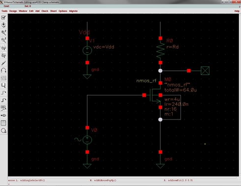
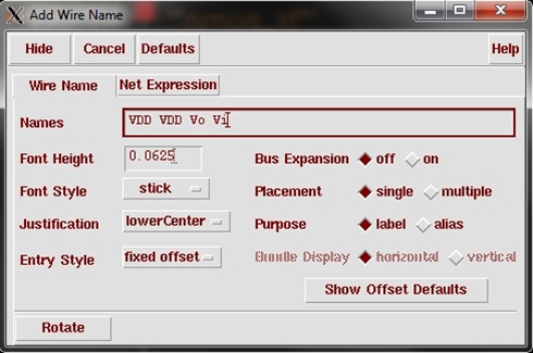
- Finally, let's add wire labels to the two stubs to "connect" them and name the input/output nets. Press "l" for the label and type "VDD VDD Vo Vi" in the "Names" box. The default settings should be fine. Then, click on the appropriate nets to name them (see schematic below).
- "Check and Save" your design: "Shift + x"

MICS IAP Members


