

Recent Publications
Journal Publications (January 2012 - December 2012)
Low-Voltage Low-Power 1.6 GHz Quadrature Signal Generation through Stacking a Transformer-Based VCO and a Divide-by-Two
Shen Wang, Vipul Chawla, Dong Sam Ha, Fellow, IEEE, and Beomsup Kim, Fellow, IEEE
(IEEE Transactions on Circuits and Systems – I: Regular Papers, Vol. 59, No. 12, December 2012)
Abstract — In this paper we present a differential VCO stacked with a divide-by-two to generate quadrature signals for low-power wireless applications. The transformer-based VCO core adopts the Armstrong VCO configuration to mitigate the small voltage headroom and the noise coupling. The operating conditions of the proposed quadrature local oscillator (LO) circuitry are derived based upon a linearized small-signal model. Also the phase noise performance is analyzed using a frequency-domain approach. The analytical results indicate that the mutual inductance and the quality factor of the primary coil play an important role in the trade-off between power and noise. The proposed LO was fabricated in 65 nm CMOS technology. The LO operates at 1.6 GHz under 1 V supply voltage and consumes only 2.6 mW of power. The measured phase noise is -140.3 dBc/Hz at 10 MHz offset frequency.

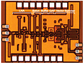
An Improved Wideband All-Pass I/Q Network for Millimeter-Wave Phase-Shifters
Sang Young Kim, Student Member, IEEE, Dong-Woo Kang, Member, IEEE, Kwang-Jin Koh, Member, IEEE, and Gabriel M. Rebeiz, Fellow, IEEE
(IEEE Transactions on Microwave Theory and Techniques, Vol. 60, No. 11, Nov. 2012)
Abstract—This paper presents the design and analysis of an improved wideband I/Q network and its implementation in a wideband phased-array front-end. It is found that the addition of two resistors (Rs) in the all-pass I/Q network results in improved amplitude and phase performance versus capacitance loading and frequency, which is essential for wideband millimeter-wave applications. A prototype 60–80 GHz phased array front-end based on 0.13 um SiGe BiCMOS is demonstrated using the improved quadrature all-pass filter (QAF) and with 4-bit phase shifting performance at 55–80 GHz. Application areas are in wideband millimeter-wave systems.
A Tunable Planar Inverted-F Antenna for Digital Video Broadcast-Handheld Applications
Majid Manteghi, Member, IEEE
(Microwave and Optical Technology Letters, Vol. 54, No. 11, Nov. 2012)
Abstract—A compact varactor-tuned planar inverted-F antenna is introduced for digital video broadcast-handheld (DVB-H) applications. The antenna size is 20 _ 40 _ 5 mm3, making it particularly suitable as an internal antenna. A full-wave simulator is used to calculate the scattering matrix of the antenna as a two port network. A circuit model including the two-port antenna and its tuning circuitry is simulated using a circuit simulator. The simulation results show that the antenna is continuously tunable within the entire frequency range of the DVB-H standard, 470–702 MHz. The antenna is prototyped and tested. The measured results are in agreement with the simulation data.
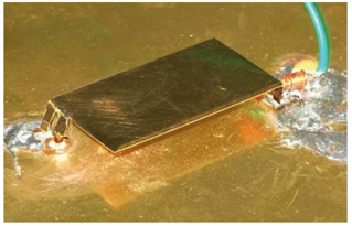
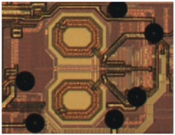
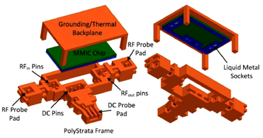
Liquid-Metal Vertical Interconnects for Flip Chip Assembly of GaAs C-Band Power Amplifiers Onto Micro-Rectangular Coaxial Transmission Lines
Parrish Ralston, Student Member, IEEE, Marcus Oliver, Member, IEEE, Krishna Vummidi, Member, IEEE, and Sanjay Raman, Senior Member, IEEE
(IEEE Journal of Solid-State Circuits, Vol. 47, No. 10, Oct. 2012)
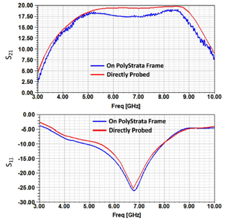
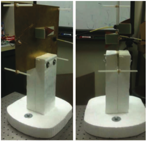
Abstract—Prior work has demonstrated a new process utilizing room-temperature liquid metal, Galinstan, as an interconnect material for flip-chip bonding. This interconnect forms a flexible bond between chips and carriers, and, therefore, a flip-chip assembly using this technology is much less susceptible to thermomechanical stresses. This paper applies this concept to interconnect GaAs MMIC chips to 3-D Polystrata transmission-line structures. Passive assemblies are utilized to model, test, and verify liquid–metal interconnections, giving average losses per liquid–metal transition of about 0.11 dB out to 26.5 GHz, low parasitics per transition, and demonstrated reliability after temperature cycling. A prefabricated GaAs MMIC chip is postprocessed for liquid–metal assembly. Measured results show, over theMMIC’s 4.9–8.5-GHz frequency range, the system’s overall reduction in gain of the MMIC is 1.4 dB or 0.7 dB per RF transition as compared with direct probing of the MMIC chip.
Application of Singularity Expansion Method for Monitoring The Deployment of Arterial Stents
Majid Manteghi, Member, IEEE, Daniel B. Cooper, and Pavlos P. Vlachos
(Microwave and Optical Technology Letters, Vol. 54, No. 10, Oct. 2012)
Abstract—A stent is a metal tube used to treat blocked blood vessels in the body. The stent is deployed into obstructed part of the blood vessel to keep it open and improve the blood flow in the diseased area. During the stent implantation, the collapsed stent is expanded into the artery to a size so as to stick to the artery walls. Because of the significant health dangers caused by the over-expansion or under expansion of the stent, having a proper estimation of diameter of the stent in the artery during expansion is important. However, yet to date, no method exists that would allow real time monitoring during and after the stent expansion process. In this article, we present a novel methodology to estimate diameter of the stent during and after deployment in the artery by applying the singularity expansion method (SEM). According to SEM, the transient electromagnetic signal scattered from bodies can be described by poles and residues. Poles are intrinsic property of the body that can be used to detect deformation of an object such as expansion. We have demonstrated the idea of estimating diameter of a stent via tracking poles by both simulation and measurement.
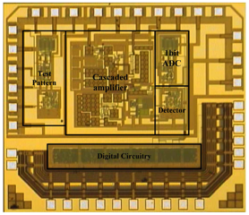
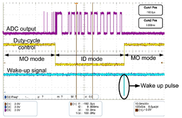
A New Approach to Low-Power and Low-Latency Wake-Up Receiver System for Wireless Sensor Nodes
Dae-Young Yoon, Chang-Jin Jeong, Justin Cartwright, Ho-Yong Kang, Seok-Kyun Han, Nae-Soo Kim,
Dong-Sam Ha, Fellow, IEEE, and Sang-Gug Lee, Member, IEEE
(IEEE Journal of Solid-State Circuits, Vol. 47, No. 10, Oct. 2012)
Abstract—A new wake-up receiver is proposed to reduce energy consumption and latency through adoption of two different data rates for the transmission of wake-up packets. To reduce the energy consumption, the start frame bits (SFBs) of a wake-up packet are transmitted at a low data rate of 1 kbps, and a bit-level duty cycle is employed for detection of SFBs. To reduce both energy consumption and latency, duty cycling is halted upon detection of the SFB sequence, and the rest of the wake-up packet is transmitted at a higher data rate of 200 kbps. The proposed wake-up receiver is designed and fabricated in a 0.18 μm CMOS technology with a core size of 1850x1560 μm for the target frequency range of 902–928 MHz. The measured results show that the proposed design achieves a sensitivity of 73 dBm, while dissipating an average power of 8.5 μWfrom a 1.8 V supply.
Low-Power Design of a Self-powered Piezoelectric Energy Harvesting System With Maximum Power Point Tracking
Na Kong, Student Member, IEEE, and Dong Sam Ha, Fellow, IEEE
(IEEE Transactions on Power Electronics, Vol. 27, No. 5, May 2012)
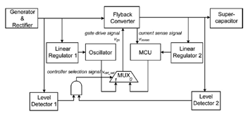
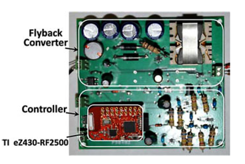
Abstract—A low-power energy harvesting system targeting to harvest several milliwatts from vibration is presented in this paper. Several low-power design schemes to reduce power dissipation of the proposed system are described, and sources of power loss are analyzed to improve the power efficiency. A discontinuous conduction mode (DCM) flyback converter with the constant on-time modulation is adopted for our system. The DCM operation of a flyback converter is chosen as for maximum power point tracking (MPPT) to be implemented with a single current sensor. The constant on-time modulation lowers the clock frequency of the controller by more than an order of magnitude for our system, which reduces the dynamic power dissipation of the controller. MPPT, executed by a microcontroller unit (MCU), is achieved through dynamic resistive matching, and the MPPT is executed at intermittent time intervals due to a relatively slow change of the operating condition. When MPPT is not active, the MCU operates at a lower clock frequency to save power. Experimental results indicate that the proposed system harvests up to 8.4 mW power under 0.5-g base acceleration with four parallel piezoelectric cantilevers and achieves 72% power efficiency around the resonant frequency of 47 Hz.
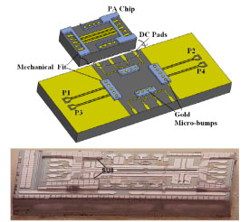
Vertical RF Transition With Mechanical Fit for 3-D Heterogeneous Integration
Lihan Chen, Student Member, IEEE, JosephWood, Student Member, IEEE, Sanjay Raman, Senior Member, IEEE, and N. Scott Barker, Member, IEEE, John Marcus Oliver, Member, IEEE
(IEEE Transactions on Microwave Theory and Techniques, Vol. 60, No. 3, March 2012)
Abstract—This paper presents the design, simulation, and measurement of a vertical RF interconnect with mechanical fit for 3-D heterogeneous integration. The mechanical fit is a flip-chip strategy employing interlocking SU-8, an ultra-thick photoresist, structures to prevent misalignment during assembly and increase the reliability of the interconnects. To determine the electromagnetic characteristics, such as insertion loss and the coupling between face-to-face chips, different test structures were fabricated and measured. Experimental results show excellent RF performance up to 110 GHz with low insertion loss (better than 0.1 dB per transition at 40 GHz).
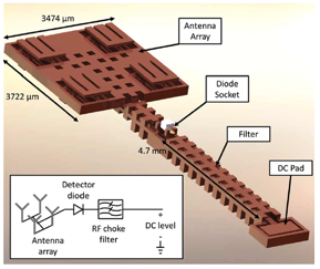
A W-Band Micromachined 3-D Cavity-Backed Patch Antenna Array With Integrated Diode Detector
John Marcus Oliver, Member, IEEE, Jean-Marc Rollin, Member, IEEE, Ken Vanhille, Member, IEEE, and Sanjay Raman, Senior Member, IEEE
(IEEE Transactions on Microwave Theory and Techniques, Vol. 60, No. 2, Feb. 2012)
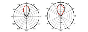
Abstract—A2×2 array of -band air-dielectric cavity-backed patch antennas is presented. The array and its components are fabricated using a sequential surface micromachining technique known as the Polystrata process. Each antenna has a simulated 4.1% 10-dB return-loss bandwidth of about 94.5 GHz, a radiation efficiency of 95%, and a gain of 8.3 dB at broadside with a 76 3-dB beamwidth. The simulated gain of the entire array is 13 dB. To facilitate system integration and measurement, several methods of interface are explored, including ground–signal–ground probing, direct transition to WR-10 waveguide, and hybridly integrated detector diodes. A measured return loss of 32 dB at 94 GHz with a 10-dB bandwidth of 3.25GHz is measured for a single antenna, and 18 dB with a 10-dB bandwidth of 4.6 GHz is measured for an array. Measured E- and H-plane 3-dB beamwidths of 25 are reported. Antenna pattern measurements show good correlation with simulated results. The measured broadside gain for the antenna array is 13.5 dB at 94 GHz.

MICS IAP Members


