

Introduction to Antenna, Analog, RF labs
Analog IC Lab
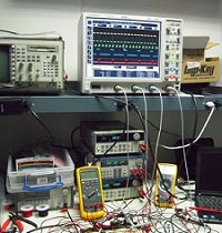
The research thrust of the analog IC lab is analog and mixed-signal IC design and system prototyping. Current research activities include energy harvesting, a wireless motion sensor for fall prevention, high speed fiber optic communications, and power line communications. The analog IC lab designs and fabricates prototype systems with off-the-shelf components as well as our own chips.
Research on Energy Harvesting
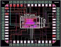
Our research targets energy harvesting in the range of sub-miliwatts to ten watts, depending on application, from solar, thermal, and vibration sources. The fluctuation and intermittence of ambient energy sources poses a technical challenge to harvest maximum energy. Maximum power point tracking (MPPT) dynamically matches the load impedance to the source impedance for maximum power transfer. Currently, we are investigating design of a power management IC, in which an MPPT algorithm is implemented with an analog circuit operating in the subthreshold region. The ultimate goal of this research is development of a power management IC for multi-source energy harvesting, which can be applied to various small scale energy harvesting sources such as indoor light, body heat, human motion, and Wi-Fi RF radiation.
Another research topic is to investigate wideband vibration energy harvesting. Wideband vibration energy is abundant in nature and comes from many sources such as human motions, industry machines, and automobiles. We developed a power management circuit (PMC) which implements an MPPT algorithm to match the source resistance dynamically. Our PMC is low power, but the efficiency drops sharply at off resonant frequencies and is not suitable for wideband vibration energy harvesting. To address the problem, we are investigating a variation of complex conjugate matching, which is tailored for wide bandwidth vibration energy. We are also collaborating with a mechanical engineering team to harvest vibration energy from railcars to power wireless sensor nodes. The target power of our energy harvester is 10 W.
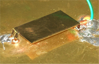
A light energy harvesting research topic is to develop a wearable solar jacket with an array of solar panels and distributed PMCs. Irradiance of the solar panels on a solar jacket changes rapidly and can be partially shaded. We are investigating design of a solar jacket system to maximize the amount of power harvested.
Development of Wireless Motion Sensors to Monitor Elders in Health Care Facilities
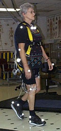
Recent efforts to improve fall detection in the elderly population can help prevent the nightmare scenario of an injured loved one lying helplessly for an extended period. However, once a fall has occurred, outcomes are typically poor and costs are high, regardless of how quickly caretakers detect and respond to falls. Fall prevention is therefore a key to health preservation. The research investigates development of a portable fall prediction monitoring system for early detection of fall risks that can provide data for diagnosis / treatment before a fall occurs to reduce long-term health effects and injuries. Users would wear the device as a faux piece of jewelry, on clothing, or around an ankle. It will measure small declining increments in gait, posture, and mobility of a patient, all of which are major indicators of a future fall.
The research project involves four different teams across different disciplines, Prof. Thurmon Lockhart (PI, Industry and Systems Eng.), Prof. Karen Roberto (Center for Gerontology), and Prof. John Lach (Electrical and Computer Eng., Univ. of Virginia), and is funded by NSF's Smart Health and Wellbeing Program ($1.2M for four years). Our team develops a wearable wireless sensor node, which senses the motion of a person and transmits the data to a host computer wirelessly. The major design objective is to reduce the power dissipation of the sensor node without compromising the quality of key data captured.
Antenna Lab
The research thrust of the antenna lab is antenna and feed network theory, design, prototyping, and measurement. Current research activities include but not limited to: electromagnetics theory, ultra-wideband and impulse radiating antennas, electrically small antennas, nonlinear time-variant antennas, reconfigurable antennas, phased arrays, wireless power transfer, space-time-frequency target identification techniques, conventional and chipless RFID.
Non-LTI Antennas
Conventional approaches to antenna design depend on linear time invariant (LTI) techniques which have proven practical and effective, but they also impose inherent design limits. It has been shown that antenna size determines quality factor, which is called fundamental limits of antennas. There are other limitations on gain and bandwidth which are all based on LTI systems.
We have demonstrated that a new approach – design and analysis of systems using nonlinear or time-variant components – has the potential to dramatically expand the design space while still meeting performance requirements, with potentially transformative impact in areas such as antenna miniaturization and filter design. The goal of this research is to build on promising preliminary results to further develop techniques for design and analysis of nonlinear and/or time-variant (non-LTI) antennas and to assess their performance characteristics.
We have been creating theoretical bases and simulation tools required to analyze and design both nonlinear and time-variant antennas. We have also prototyped a tunable antenna and used it as a time variant-antenna.
Chipless RFID and Space-Time-Frequency target identification techniques:
The objective of this research is to formulate the analytical tools and practical techniques necessary to explore a new class of RFID tags with no semiconductor devices (chipless RFID tags). In essence, a chipless RFID is a structure that scatters a unique signature when excited which is inherent to the structure. Data is encoded as natural resonances in the structure and retrieved from the scattered-field data. Data retrieval is based on Singularity-Expansion-Method (SEM) analysis in the complex-frequency domain using target identification techniques. The research will commence with a fundamental design, incorporating SEM principles into comprehensive analysis, simulation, and measurements. The results provide the theoretical basis for the behavior of chipless RFIDs. Data embedding techniques developed from the fundamental structure will be used to devise tags with a higher data density. Furthermore, the techniques will be extended to more arbitrary structures and include structural interactions.
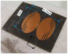
Our first design was an elliptical dipole with three slits which include 3 poles. We have been working on detection techniques and new tag design in parallel. Our new design is a 25mm diameter disc with 22 poles. We have also developed a novel space-time-frequency detection technique to identify the tag and its position in 3D space.
Wireless power transformation
A rise in the need for dynamic energy allocation has been associated with the saturation of available portable wireless electronic devices. More significantly, implanted devices need high efficiency, miniaturized, wireless power transfer devices to ease recharging their batteries. Currently, the methods for transmitting this energy efficiently have been limited to a number of options, including near field resonant magnetic coupling. Previous research with mid-range (D ≈ 4R) wireless power transfer has resulted in coupling efficiencies of close to 40%.
We have been able to create a hybrid simulation to optimize the near-field coupling structure to achieve its maximum possible coupling efficiency. Our results guide us to reach the optimum design for near field couplers to increase coupling efficiency.
Course: Antennas and Analog IC Tracks
Novel techniques in phase array design
Phased arrays have always been attractive to many different applications. Due to the high manufacturing cost, only military and government organizations were able to afford the technology. Recently, there have been numerous commercial applications for phased arrays which require low price phased arrays. This has opened a new area of research to design and prototype low price phased arrays. We have introduced a novel sampling methodology to simplify a digital phased array which results in a reduction of the number of front-end components, relaxed ADC requirements, and reduced the processing cost.
RF Lab
The research thrust of RF lab is integrated circuits and systems design for wireless and wireline communications ranging from RF to microwave, millimeter-wave and sub-millimeter wave frequency regimes. Recent research efforts include integrated radar systems on a silicon chip for passive and active imaging and remote sensing applications. We are also pursuing digitally-enhanced RF design techniques to improve performance, power efficiency, and multi-functionality.
Research on Integrated Phased Arrays on Silicon Technologies
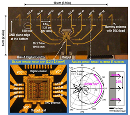
Phased-array antenna is a smart antenna system providing agile electromagnetic beam control in space domain, and has been widely used for defense radar systems over the last decades. Traditionally phased array transmitter and receiver systems have been built with III-V technologies in a discrete hybrid-integration at a board level. Recently there have been active research efforts to realize fully integrated phased array electronics in search for a low-cost system solution, yet providing more versatile and adaptive beam control capability. Our RF Lab has demonstrated a fully integrated 6-18 GHz phased array receiver in SiGe BiCMOS technology with complete system level verifications on an array antenna board (shown below), which has been successfully transferred to main US DoD industry for the development of advanced defense radar systems. We also demonstrated 16-element integrated phased array transmitter at 44 GHz, featured as one of the first and the most highly integrated phased array electronics in silicon technologies at millimeter-wave frequencies. Our current research effort is in a search for a wideband phased array technology in combination of analog and digital beam forming techniques that can operate over a 10:1 bandwidth in 0.4-20 GHz of frequency range. We are also pursuing our active research on millimeter-wave phased array transceivers (94~120 GHz) for potential uses in radar remote sensing and wireless point-to-point communications.
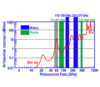
Research on Millimeter-Wave and Submillimeter-Wave Electronics
A phased-array is a smart antenna system providing agile electromagnetic beam control in space domain, and has been widely used for defense radar systems in past decades. Traditional phased array transmitter and receiver systems have been built with III-V technologies in a discrete hybrid-integration at a board level. Recently there have been active research efforts to realize fully integrated phased array electronics in search of a low-cost system solution, yet providing more versatile and adaptive beam control capability. Our RF Lab has demonstrated a fully integrated 6-18 GHz phased array receiver in SiGe BiCMOS technology with complete system level verifications on an array antenna board (shown below), which has been successfully transferred to main US DoD industry for the development of advanced defense radar systems. We also demonstrated 16-element integrated phased array transmitter at 44 GHz, featured as one of the first and the most highly integrated phased array electronics in silicon technologies at millimeter-wave frequencies. Our current research effort is a search for a wideband phased array technology in combination of analog and digital beam forming techniques that can operate over a 10:1 bandwidth in 0.4-20 GHz of frequency range. We are also actively researching millimeter-wave phased array transceivers (94~120 GHz) for potential uses in radar remote sensing and wireless point-to-point communications.

MICS IAP Members


